
How COB LED Displays Achieve High Brightness, High Contrast, and Low Power Consumption.
On the path toward ultimate visual performance for COB displays, surface treatment is a core factor that shapes image texture, reliability, and energy efficiency. The evolution of LED surface finishing is a continuous journey of solving industry pain points. For a long time, the industry had to make trade-offs between off-state black level, output brightness, power draw, and long-term reliability. Traditional processes often compromised one performance metric for another: a deep black background came at the cost of brightness, boosting brightness led to higher power consumption, and enhanced protection risked introducing harmful mechanical stress to LED chips. Through iterative upgrades of materials and structural design, COB surface solutions have evolved from full epoxy encapsulation to composite optical stacks. VISIONPI’s self-developed 3rd-generation nano-black surface treatment technology marks a key milestone along this technological roadmap.
When pursuing superior picture quality for COB LED walls, the surface finishing process directly determines visual performance, durability, and power efficiency. The upgrade of COB surface technology is essentially engineers tackling the limitations of older solutions, and it has gone through three major generations.
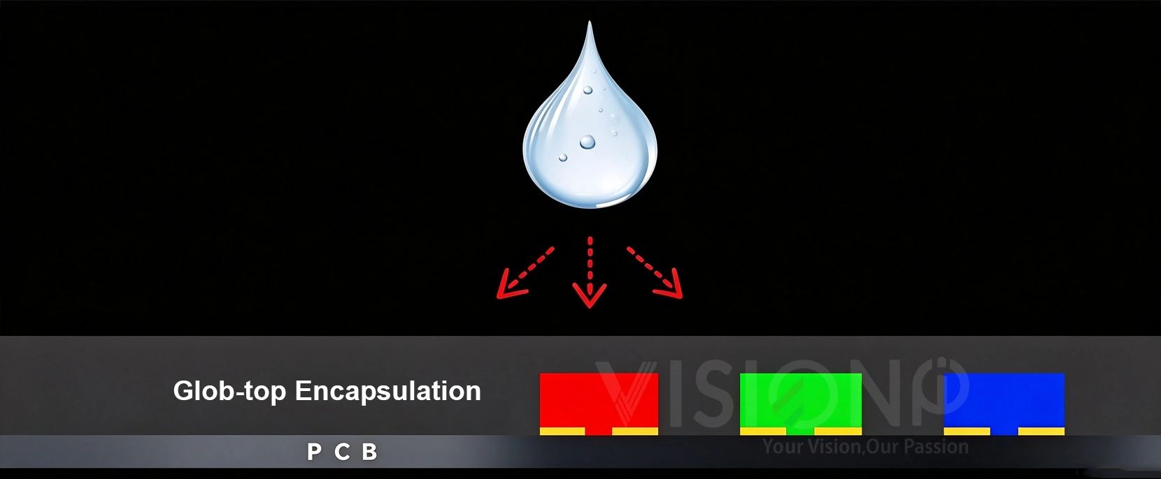
Generation 1: Epoxy Glob-Top Coating (Early Traditional Solution)
-
Early COB displays used epoxy glob-top coating. A thick, rigid epoxy resin fully encapsulates and buries the LED chips.
Many customers wonder why this encapsulation method is prone to chip damage. After curing, the epoxy becomes hard and brittle. It shrinks as it transitions from liquid to solid. Combined with repeated thermal cycling as the screen turns on and off, the rigid glue and LED chips expand and contract at different rates. Deformation stress concentrates on the tiny chips. It is similar to embedding a glass bead firmly inside cement. When the cement shrinks and deforms, the bead can easily crack, triggering chip failure, dead pixels, and lower production yield.
Besides reliability risks, this process has other drawbacks. The adhesive tends to yellow over time, gradually ruining the screen’s deep black background. It is also hard to control glue thickness consistently. Uneven coating creates an irregular surface and patchy, inconsistent black levels across the panel. These limitations make this old solution unsuitable for high-end projects demanding uniform image quality.
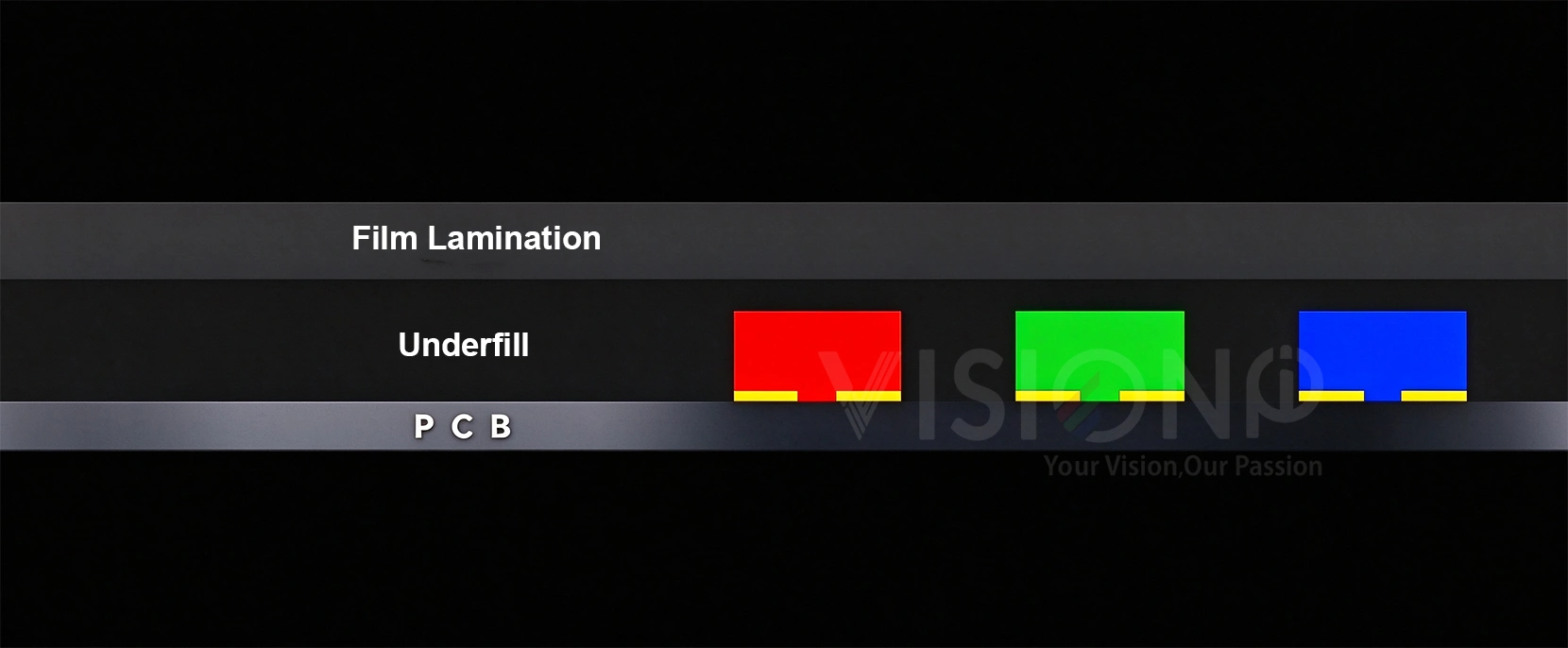
Generation 2: Underfill Adhesive + Black Lamination Film (Widely Used COB Solution)
The industry upgraded to the “underfill adhesive + surface black film lamination” structure to resolve material and reliability issues from the first generation.
Unlike full-encapsulation epoxy glob-top, underfill adhesive does not cover the light-emitting top of chips. It flows by capillary action into the narrow gaps between LED chips and the PCB substrate, with controlled wicking along chip sidewalls. Formulated with a flexible modified polymer, it builds an elastic buffer around the bottom and sides of chips. When the PCB bends slightly under heat, the flexible underfill absorbs and disperses mechanical stress, preventing stress concentration on chip solder joints and greatly improving chip stability. The deep black tone and flat surface come from the top laminated optical black film.
However, it has an unavoidable weakness. Most black lamination films engineered for deep black performance have low light transmittance. For example, if the native chip brightness reaches 2000 nits, the black film blocks and absorbs much of the light, often dropping brightness to roughly 600 nits. To maintain acceptable brightness, the chips must run at higher power, which sharply increases power consumption. You can’t achieve deep black backgrounds, high brightness, and low power consumption at the same time.
Generation 3: Nano-Black Surface Treatment (New-Generation Premium Solution)
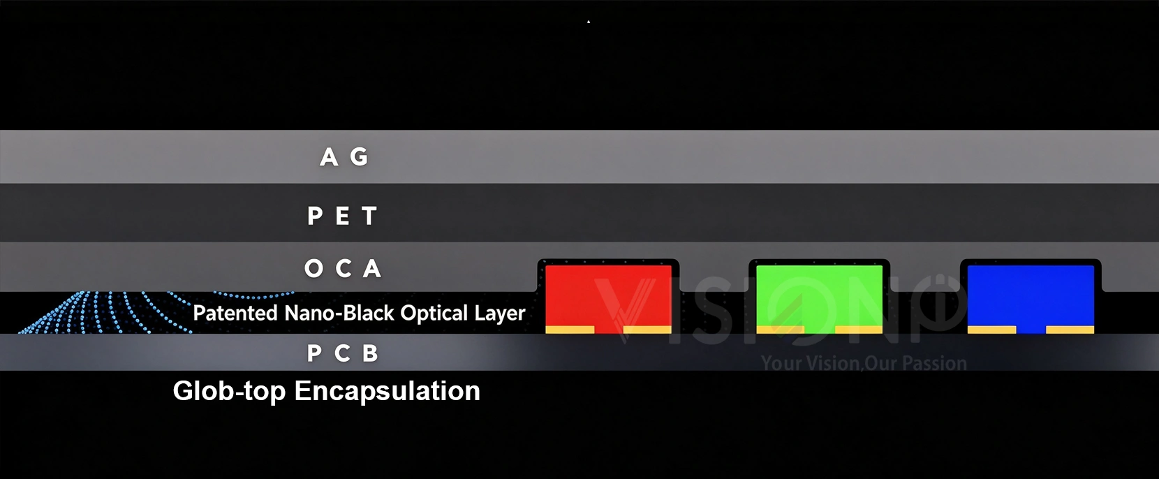
The new Nano-Black process is developed specifically to address the heavy light loss of conventional black lamination films. Instead of simply applying a single black film, it adopts a patented stacked optical structure. From bottom to top: PCB substrate, patented Nano-Black optical layer, OCA optical adhesive, PET base film, and AG anti-glare layer. Each layer serves a clear purpose:
- PCB Substrate: The printed circuit board with soldered LED chips, delivering power and image signals.
- Patented Nano-Black Optical Layer: The core of this technology. It selectively absorbs ambient stray light and external reflections. Reflections from spotlights and surrounding lighting are suppressed, while imaging light emitted by LED chips passes through with minimal attenuation. It acts like a one-way optical filter: blocking incoming environmental glare while letting the screen’s own light output outward.
- OCA (Optically Clear Adhesive): A high-transmittance special optical bonding adhesive, fundamentally different from ordinary adhesive tapes. Standard bonding glues have poor light transmission and tend to haze and trap microbubbles that degrade optical performance. OCA is nearly perfectly transparent, engineered for bubble-free lamination of optical layers. It tightly bonds the PET film to the underlying Nano-Black layer and eliminates air gaps between layers. Air interfaces cause extra reflection and reduce contrast. The full lamination technology used in smartphone and tablet screens relies on the same type of OCA material.
- PET Film (PET Base Substrate): The backbone of the optical stack. PET is a transparent polyester film with excellent toughness, tear resistance, and dimensional stability. The AG coating is applied onto this PET film, providing a stable carrier for the top optical functional layer.
- AG (Anti-Glare Layer): The outermost matte coating, similar to the anti-glare surface on laptop screens. Glossy surfaces create sharp, distracting mirror-like glare when hit by spotlights. The AG layer features a micro matte texture to diffuse specular reflection. In exhibition halls and conference rooms with strong ambient lighting, it eliminates bright hotspots so visuals stay clear and undisturbed.
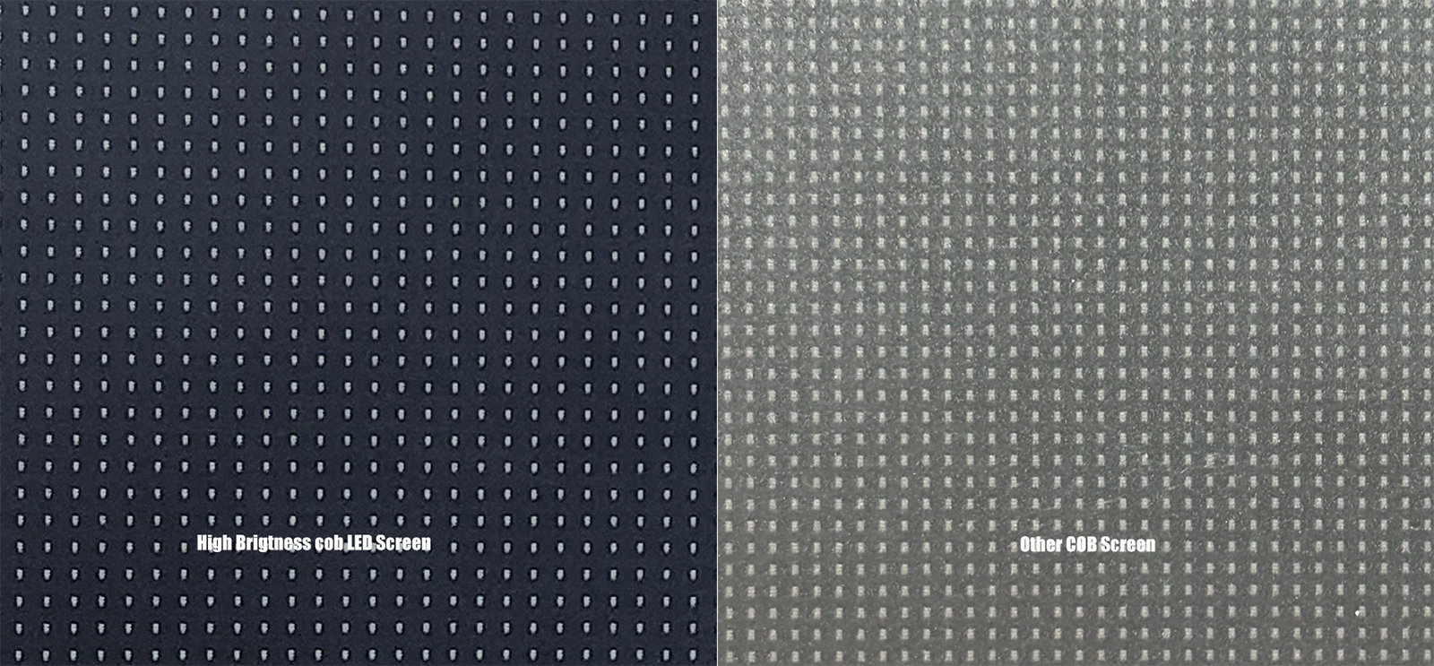
Higher Brightness
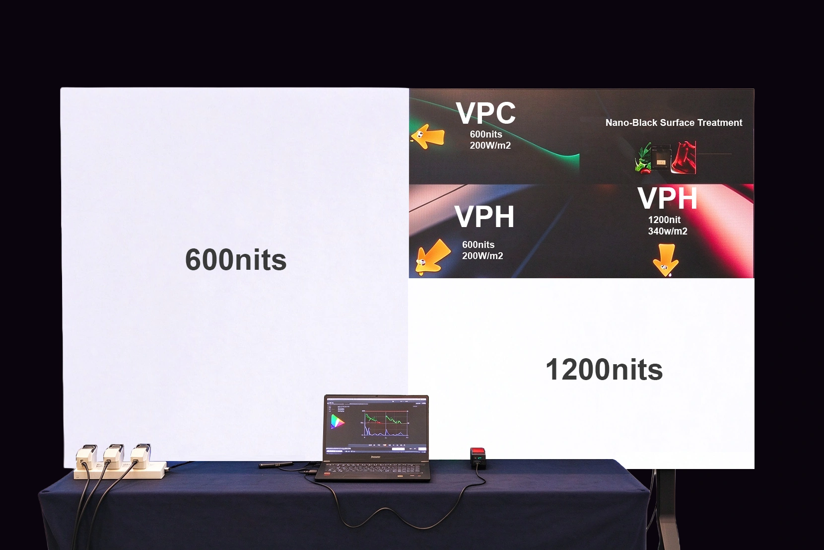
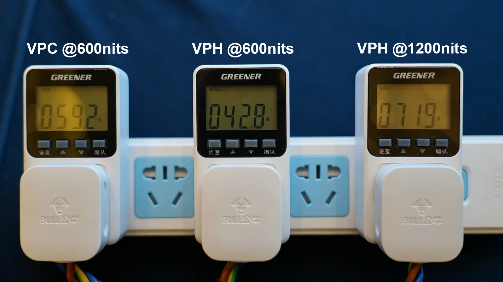
At 600 nits (daily operation), VPH series consumes only 210W/㎡, cutting power use by 30% vs standard COB displays and lowering running electricity costs. At 1200 nits for high-brightness professional use, its 350W/㎡ power level matches competitors. It offers excellent cost efficiency, saving energy in normal operation while preserving full high-brightness performance.
Outstanding display performance comes from continuously refining materials and manufacturing processes. Sustained R&D investment and mature mass-production capability back Nano-Black technology. With this new-generation surface treatment, VISIONPI continues to push the performance boundaries of COB direct-view LED displays and delivers reliable, top-tier solutions for premium commercial applications.
Reach out now and let’s build your next premium LED display project.