What is Mip LED Display
TrendForce research data shows that the LED small-pitch display screen market will reach US$4.232 billion in 2022, a growth of 12% compared with the same period of time. In addition, against the backdrop of the Russian-Ukrainian conflict and inflation, the overall demand for LED displays shrank last year, and display manufacturers have been more active in promoting ≤P1.0 mini/micro led screen.
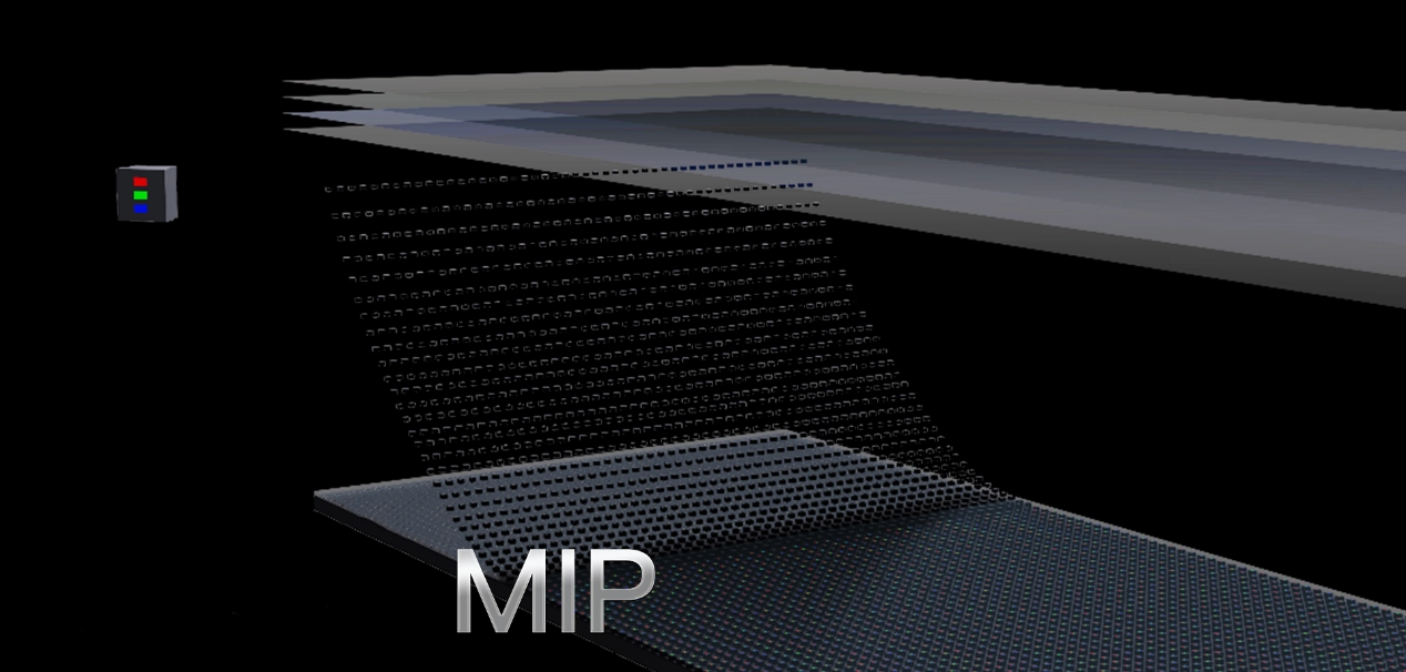
History of LED display package technology:
The development of LED screen package technology from DIP to SMD to IMD to COB is a process of innovation and improvement in response to market demand and technological progress.
- DIP stands for Dual In-line Package. It is the oldest and simplest packaging method, which involves inserting two pins of each LED chip into a plastic holder and soldering them to the PCB board. DIP packaging has the advantages of high brightness, good heat dissipation, and low cost, but it also has the disadvantages of large size, low resolution, and poor color uniformity. DIP packaging is mainly used for outdoor displays with large pixel pitches.
- SMD stands for Surface Mounted Device. It is the most widely used packaging method in the current LED display industry, which involves fixing the LED chips on a bracket, connecting them with gold wires, and protecting them with epoxy resin. The SMD package can integrate red, green, and blue LED chips into one lamp bead, which can be soldered to the PCB board by reflow soldering. SMD packaging has the advantages of small size, large viewing angle, good color mixing, and high reliability, but it also has the disadvantages of low brightness, poor heat dissipation, and high cost. SMD packaging is mainly used for indoor displays with small pixel pitches.
- IMD stands for Integrated Matrix Device. It is a relatively new packaging method that combines the advantages of SMD and COB. It uses surface mount technology to fix the LED chips on a metal substrate and then covers them with a transparent resin film. The IMD package can achieve a smaller pixel pitch than SMD and also has better protection, heat dissipation, and contrast than SMD. However, IMD packaging still faces some challenges such as high cost, complex processes, and low yield.
- COB stands for Chip on Board. It is another emerging packaging method that directly mounts the LED chips on the PCB board and then encapsulates them with epoxy resin or silicone gel. The COB package can achieve a very small pixel pitch, even reaching the level of mini LED and micro LED. It also has excellent protection, heat dissipation, contrast, and reliability. However, COB packaging also has some drawbacks such as high cost, difficult repair, and color inconsistency

What is Mip LED Display
Mip Stands for “Micro LED in Package”, it is a new packaging technology based on Micro LED, which can be diced into small pieces package from a micro/mini led panel, and then perform separate packaging and testing, and becomes a Mip Modules via SMT ,thereby improving the yield and reducing the cost.
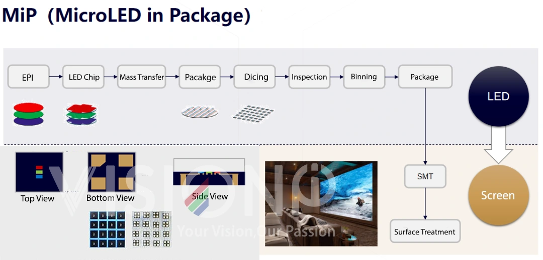
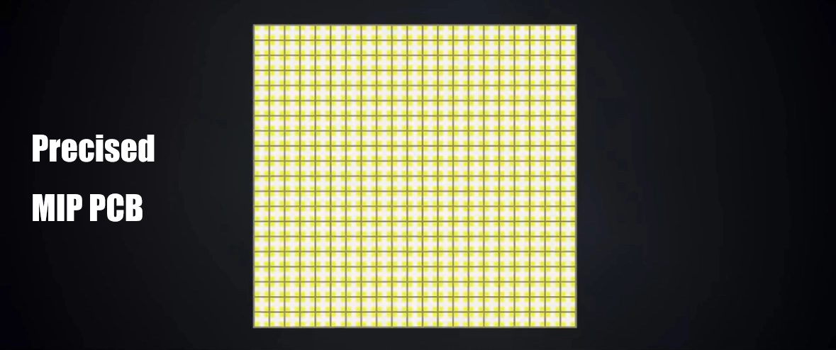
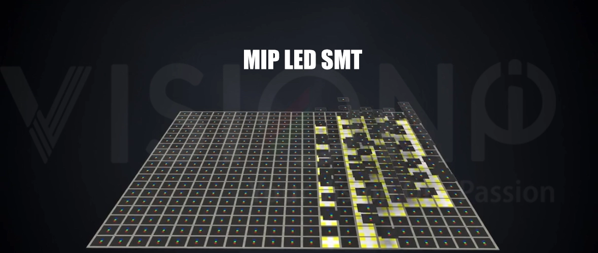
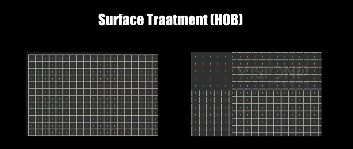
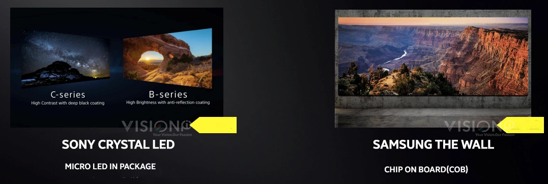
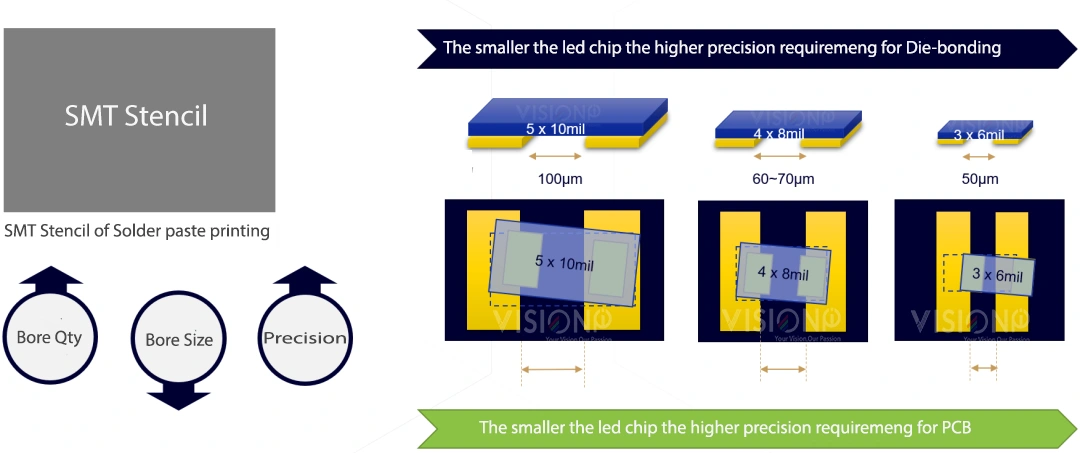
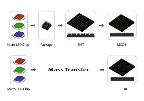
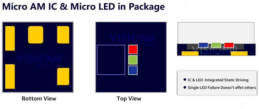

AMiP (AM IC & Micro LED in Package).
AMiP stands for “AM IC & Micro LED in Package”. It integrates the active driver IC and Micro LED chips within a single package, thus creating a “light-driver unity.” Compared to the first generation of MiP, AMiP achieves significant performance improvements. The structure of AMiP involves a Micro LED device that is 300μm x 300μm in size, using Micro LED chips smaller than 34μm x 58μm. The driver IC is positioned beside the red, green, and blue (RGB) Micro LED chips, and like MiP, it employs a fan-out pin design.
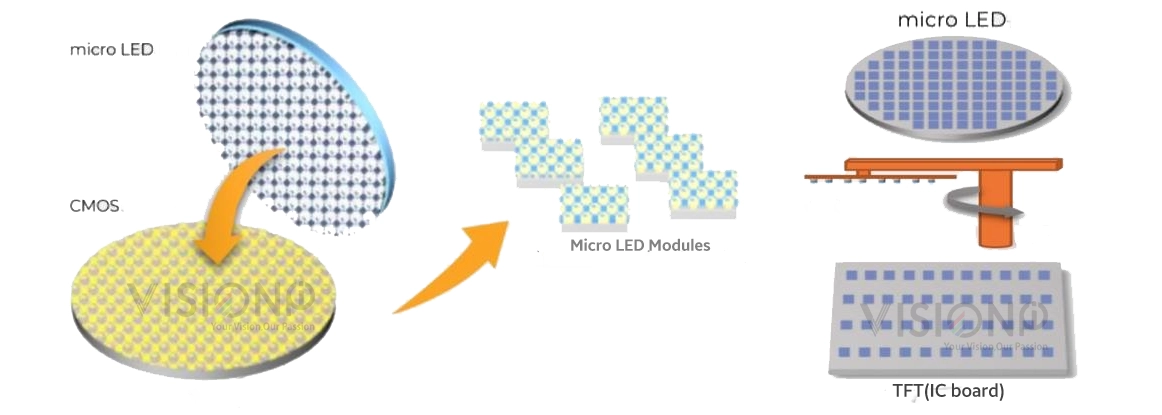

Key Advantages of AMiP:
- Flicker-Free Performance: AMiP integrates an active driver IC that eliminates flickering, which is common in traditional LED drivers, thus improving the overall display quality.
- Superior Contrast: Combining the AM driver with Micro LED’s inherent contrast advantages, AMiP can deliver superior display performance with enhanced brightness and more vivid colors.
- Simplified Circuitry and PCB Optimization: The integration of the driver IC within the package allows for simpler circuit designs, which reduces the complexity of PCB design. This simplification helps reduce PCB costs while also improving product stability.
- Addressing Traditional Driver Issues: AMiP eliminates common issues such as the “caterpillar effect”, low grayscale coupling, and flickering, resulting in a more stable and high-quality display.
- Cost Efficiency: In the development of Micro LED technology, the comparison of costs between MiP and COB (Chip on Board) is evolving. It is no longer just about comparing the price of MiP components and COB chips; the comparison now includes the cost of MiP + Micro IC versus COB + PM-IC. The packaging cost in MiP can be absorbed into the driver section, making it a cost-effective solution.
- Smaller Micro LED Chips: MiP technology benefits from the use of smaller Micro LED chips, resulting in higher contrast and greater potential for cost reduction. With ongoing price reductions in Mini RGB chips, MiP technology is gaining increasing attention from end users.

