COB VS FLIP-CHIP COB LED Display

In the field of LED display, with the development of upstream packaging technology, there gradually form two different LED display panel preparation technologies, SMD ;IMD; COB. We can use these two technologies to produce small-spacing mini LED display screens. And we will share some information about these two technologies with you.

What is COB?

COB (Chip on Board) is a kind of LED display packaging technology. LED light-emitting chips are directly bonded to the module board with high precision and connected to driver components on the module board through special media for overall protection of the light-emitting surface. COB packaging eliminates the two key procedures of turning LED chips into lamp beads and reflow soldering as compared to standard SMD packaging. 


Features Of COB LED DISPLAY

1. With Ultra-High Reliability

COB technology eliminates the process flow of SMD light-emitting tube packaging, color separation, taping, and patching, simplifies and improves the reliability of the product production process. Longer Life Span: Without the holder, the LED chip has lower heat resistance, largely increasing its life span

2. Smaller Pixel Pitch allowed

Smaller Pixel Pitch: the pitch of SMD is P1.2-P2.0, while COB is P 0.5-P2.0 .The COB technology  is not limited by the physical size, bracket, and lead of the SMD LED package, and can break through the SMD pitch limit, achieve higher pixel density, and have a more flexible dot pitch design.

3. Larger Viewing Angle: 

COB more likes the surface light source than the SMD, when light refracts, it has less light loss. COB Realizes The Conversion From “Point” Light Source To “Surface” Light Source.No pixel graininess; can effectively control the brightness of the pixel center, reduce the intensity of light radiation, inhibit moiré, glare, and glare to the retina, suitable for close and long-term viewing, not easy to cause visual fatigue, suitable for close-screen viewing.

4. Higher Protective Performance

The PCB circuit board, crystal particles, solder feet, and leads are fully sealed. The advantages of the sealed structure are an obvious-for examples, moisture resistance, anti-collision, prevention of pollution damage, and easier cleaning of the device surface.

Lateral Chip COB structure  VS A Flip-Chip COB structure

lateral chip cob vs flip chip cob

Flip chip cob led display advantages

1. Higher stability. Flip chip packaging technology eliminates wire bonding, eliminating the risk of gold wire breakage and simplifying the production process.

LED COB WIRE BONDING

2. Smaller pixel pitch.  Flip-Chip COB encapsulation is the chip-level integrated encapsulation. Without the wire bonding, the physical space size is only limited by the size of the light-emitting chip, which can achieve higher pixel density.

3. Better visual performance. Regarding display performance, the area of the Flip-Chip is smaller on the PCB board, and the duty cycle of the substrate is increased. It has a larger light-emitting area, which can present a darker black field, higher brightness, and higher contrast Presenting HDR-level display effects.

cob structrure visionpi

4. Cost-effective. There is no welding wire link, simplifying the production process and reducing equipment investment costs. As the industry scales, the product cost will be significantly reduced, especially when the dot pitch is less than 1.0mm.

Therefore, Flip-Chip COB technology is a necessary condition for the realization of MicroLED and will go further in the era of micro-display.

The Future Of direct view led display.

Flip-chip COB is an upgraded version of lateral COB, flip-chip COB improves reliability and visual performance, simplifies the production process, and narrows the pixel pitch. COB is the future of direct view led display 

COB LED VS Mini LED

The packaging technology of LED display modules can be divided into two types, one is SMD (Surface Mounted Devices) and the other one is COB (Chip On Board).  4in1 LED is still a number of SMD. The comparisons of these two products are as follows:
I. Production Cost: As compared to the flip-chip COB module, the 4in1 LED module has more production workstations (as shown in the picture below), which increases production cost. In addition, the flip-chip COB module adopts the mass transfer method to set LEDs on PCB boards; however, the 4in1 LED module applies the traditional single-chip per transfer method to set LEDs on PCB board one-by-one. Thus, the production capacity is ten to hundred times different. The cost advantage of flip-chip COB module may help speeding up the construction and expansion of virtual production environments.

As compared to the flip-chip COB module, the 4in1 LED module has more production workstations

  • II. Display Performance: In terms of display performance, the area of the Flip-Chip is smaller on the PCB board, and the duty cycle of the substrate is increased. It has a larger light-emitting area, which can present a darker black field, higher brightness, and higher contrast.COB LEDs are precisely placed on PCB boards so that the flatness and accuracy of the module are outstanding. Moreover, the viewing angle of the flip-chip COB module is around 175°, which is wider than the 160° viewing angle of the 4in1 LED module, and there is no pixel granularity on the flip-chip COB module. In addition, the flip-chip COB module can effectively suppress the moiré effect.


  • III. Product Reliability:  Flip-Chip COB can achieve true chip-level spacing, reaching the level of Micro LED. This is because, from the perspective of the LED chip, the Flip-Chip does not require wire bonding, which breaks the pixel pitch limit of the formal chip and solves the problem of metal migration in the formal LED.

    LED surface of the flip-chip COB module is packaged with an integral epoxy resin mold to avoid oxidation; the exposed solder joints of the 4in1 LED module are susceptible to interference by water and oxygen.

  • Please refer to the following comparison table of product reliability. Comparing the various characteristics, the overall reliability of the flip-chip COB module is much better. It is more suitable for the film and TV industry that requires frequent disassembly and assembly of LED modules.
flip chip cob vs mini 4 in 1 led

In summary, from the perspective of production cost, display performance and product reliability, the flip-chip COB module is significantly better than the 4in1 LED module. As an upgraded product of formal COB, flip-chip COB is based on the advantages of formal COB ultra-small dot pitch, high reliability, and non-glaring surface light source. Further, improve the reliability, simplify the production process, better display effect, perfect near-screen experience, and real chip-level spacing can be realized.

Are microLEDs the next big thing for display technology?

Are microLEDs the next big thing for display technology?

Are microLEDs the next big thing for display technology?

Sized to be individual display pixels, microLEDs are under heavy development, with emphasis on singulating, packaging, and assembling these LEDs into displays.

What is a microLED?

The term microLED typically refers to the size of the emitting area of the LED device. However, there is no clear industry clarity on the size that qualifies as “micro”—and the definition can vary based on the application. For example, for virtual-reality and augmented-reality(AV/VR) glasses, the desire is to have microLED elements that are smaller than 10 μm. For direct-view displays, some like the definition to be 50 or 100 μm. Above this size is a new category called miniLED; again, no clear emitter size range has been agreed to.

To make things even more confusing, many display companies are simply calling their latest very-fine-pitch display pixels “microLEDs” regardless of the size of the emitter being used. This is because for a display device, it is the pixel pitch (the space between full-color pixels) that is more important than the LED emitter size.

The most-familiar type of direct-view LED (DV-LED) display is a so-called “videowall.” These are modular displays made from a number of “cabinets,” with each cabinet composed of several “modules.” Each module in turn has red, green, and blue(RGB)LEDs mounted on a circuit substrate along with drivers and electrical interconnections.

Over the last few years, there has been a clear trend toward narrow- or fine-pitch LED video walls. These are generally defined as pixel pitches of under 1.5 mm, with the latest prototypes now at 0.4 mm. Such displays are designed for closer viewing distances. For perspective, 0.4 mm is very close to the pixel pitch on a 65 in. 4K-UHD resolution TV. As a result, major TV brands are very interested in this technology.

DV-LED displays can meet and often exceed LCD or OLED performance in terms of luminance, dynamic range, color gamut, viewing angle, black levels, and so on. The main disadvantage is price. One of the main cost drivers for DV-LED displays are the RGB LEDs. Moving to smaller LED emitters mean less LED device material is needed—a substantial cost reduction. The other major cost factor is the packaging of the LEDs and assembly onto the module circuit boards.

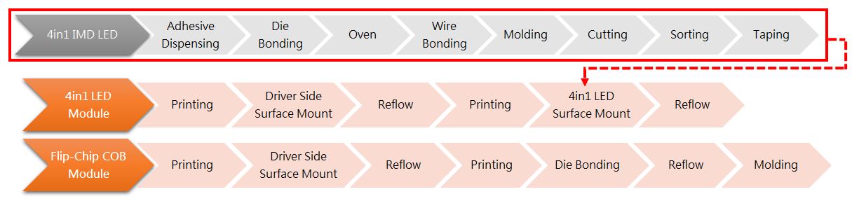
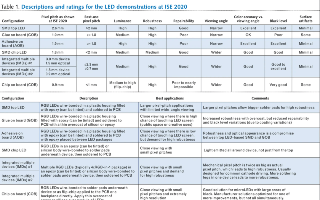
Historically, LEDs are diced from the epitaxial wafer, placed in a surface-mount package, wire-bonded in place, and encapsulated with epoxy or silicon (so-called SMD top LED). Variations in the way these LEDs are assembled on the printed circuit board (PCB) can be described as glue on board (GOB) and adhesive on board (AOB). Several newer approaches seek to reduce costs and allow smaller pixel pitches. These can be described as SMD chip LED, integrated matrix devices (IMDs), and chip on board (COB). A photo of the small-scale demo along with a table describing the configurations and strengths/weaknesses of each are shown as below:

However, it is likely that they are in the range of 100 to 300 μm in length or diameter, so either microLED or miniLED, depending on the microLED definition.

At ISE, Visionpi (Shenzhen, China) showed a state-of-the-art 0.4-mm-pitch DV-LED microLED video wall. This is a flip-chip COB approach probably to a PCB backplane. This prototype is a single-chip solution.

COB FLIP CHIP LED WALL webp

Note that the distance between each RGB set of LEDs is 0.4 mm, so the active LED diameter is around 70 μm, which is below the 100 μm microLED threshold that some use as a definition. Also note that as the active LED area gets smaller, the surrounding black area gets larger. This creates a display with a better black level and higher contrast. Sony’s Crystal LED video wall has a pixel pitch of 1.2 mm with emitters that are thought to be about 100 × 35 μm in size, leading to a display with 99% of the area being black with really great performance.

Visionpi is a company that offers display solutions to its mainly rental and staging customers. Their showcase at ISE was designed to help illustrate the difference in image quality one gets with these different packaging and manufacturing approaches. Visionpi uses a single flip-chip approach overcoated with a thin layer of adhesive silicon and black adhesive between the flip-chip devices. This display uses microLEDs with a pixel pitch of 0.83 mm and has a luminance of 2000 nits.

TV brands are also very interested in microLED technology. At CES 2020 (January 7-10; Las Vegas, NV), Samsung expanded its line of microLED-based displays called “The Wall,” while others exhibited various prototypes that they hope to bring to market in 2020 (see Table 2).

Challenges remain for all these technologies, which impacts their high costs. For example, most DV-LED displays still wire-bond the LED inside the package or to the PCB. Flip-chip devices eliminate all the wire bonding, but require that the surface of the LED epiwafer be planarized so the n and p contacts are at the same level. The device can then be flipped over to directly solder to the PCB.

Wire-bonded multi-in-one IMD devices are available today, as are single flip-chip LEDs, but they are not yet very common. IMD flip-chip devices are still only available as prototypes.

Singulating the individual die or IMD devices also has its issues, too. When a laser is used to separate the die, it can leave rough edges that reduce the black level. Overcoats of epoxy can also have thickness variations leading to variations in black level over the display. In addition, bad LEDs need to be removed and replaced in the manufacturing process, which can vary from doable to nearly impossible.

As Lucas. W, Director of LED & Displays at visionpi, noted, “Each LED videowall supplier working on COB has some unique processes to optimize cost and performance parameters. The reality is that some have optimized one set of parameters and another a different set, but none have optimized all just yet. However, the fact that most of them can be solved already makes us confident for the future of COB.”

Developing next-generation microLED manufacturing

One fundamental issue with DV-LED displays is that the LED pitch on the epiwafer is very small, while the pitch on the DV-LED display can vary widely. Current mass transfer methods can transfer one to dozens of LED chips at once. To truly become cost-competitive with LCD or OLED displays, the transfer rate must increase to millions per minute. As a result, this is where a lot of innovation is concentrated now.

The most-common approach is a stamp transfer that can pick up thousands of microLEDs at a time and transfer them to a separate substrate with a different pixel pitch. Another approach uses laser pulses to transfer LEDs from a carrier substrate to the display substrate. Few details about these and other approaches are ever revealed, as they are considered proprietary intellectual property.

The next problem to worry about is yield. Not only must the mass transfer be extremely fast, but placement must be very accurate. As the size of the microLED gets smaller and smaller, the ability to pick up and accurately place it becomes more and more difficult. If a defect is found, is there a repair process that does not take far longer to complete than the initial mass transfer time? And this just applies to mechanical/electrical yield.

All the LEDs must also fall within a certain range of luminance and wavelength to provide the kind of performance demanded by end users. This is pushing the LED wafer makers to improve the way the LEDs are fabricated. New MOCVD chambers with much better uniformity and layer control are now available to enable most of the wafer to fall within quality control guidelines. Traditional gallium nitride (GaN)-based blue and green LEDs are grown on sapphire epiwafers with a 2 to 6 in. substrate size. To lower costs, larger wafer sizes are desirable. Consequently, GaN-on-silicon epiwafers are also being used to grow green and blue microLEDs at 8 in. sizes now, with the potential to go to 12 in. wafers later.

Many of these requirements point to the need to have a way to fully characterize the microLEDs at the wafer level prior to any mass transfer method. Companies are working on this need as well.

All these LEDs also need to be driven with signal to create an image. DV-LEDs mount the LEDs on a PCB and use a lot of driver chips to send signals, and next-generation DV-LEDs may well be mounted on glass substrates with active-matrix driving using TFTs at each pixel location. This will provide better control of each microLED and can leverage the TFT-on-glass fabrication infrastructure already in place for LCD displays.

Finally, since the display needs RGB LEDs, all the above improvements and techniques must be done three times for the RGB wafers.

Subscribe To Our Newsletter

Join our mailing list to receive the latest news and updates from our team.

You have Successfully Subscribed!

Pin It on Pinterest