COB LED Display Development 2024
In 2023, the global LED market encountered significant hurdles, leading to a decrease in its market value to $12.608 billion. This decline was attributed to a combination of factors, including diminished demand from end markets, slow inventory turnover, and fierce competition over pricing. Despite these challenges, the LED industry is poised for a positive shift in 2024. According to insights from TrendForce, expectations are set for the market value to experience a growth, ascending to $13.003 billion, marking a 3% increase compared to the previous year.
One of the notable trends within the LED sector is the burgeoning demand for MiniLED (COB) video walls. This demand is being driven by top manufacturers such as Samsung, LG Electronics, Leyard, Unilumin, and Absen, indicating a robust growth trajectory in this segment.

The Evolution and Future Prospects of COB LED Display Technology in 2024
As we navigate through 2024, the landscape of LED display technology continues to be shaped significantly by the advancements and integration of Chip on Board (COB) technology. Since its emergence in 2012, COB technology has steadily transformed the direct-view LED display industry, offering unparalleled advancements in durability, resolution, and cost-effectiveness. This article delves into the current state of COB LED displays, their comparative advantages over traditional technologies, and anticipates future developments.
Core Attributes of COB LED Technology
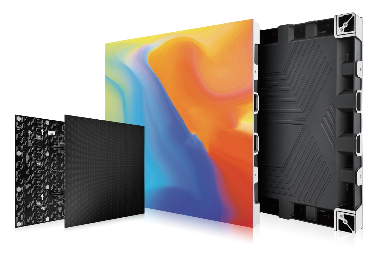
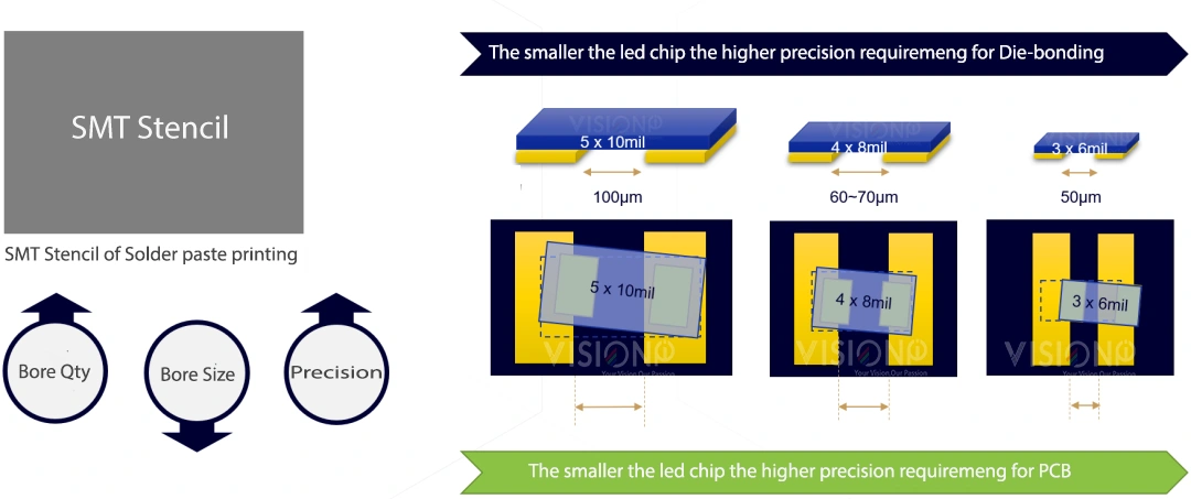
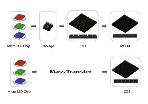
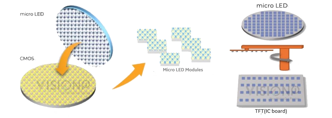
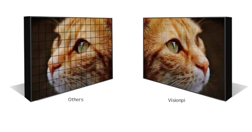
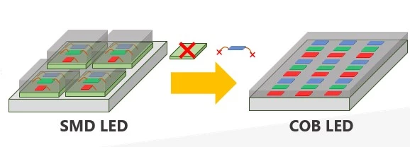
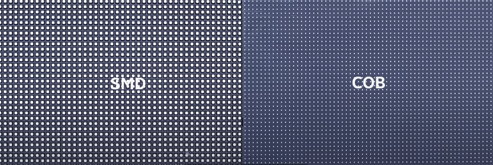
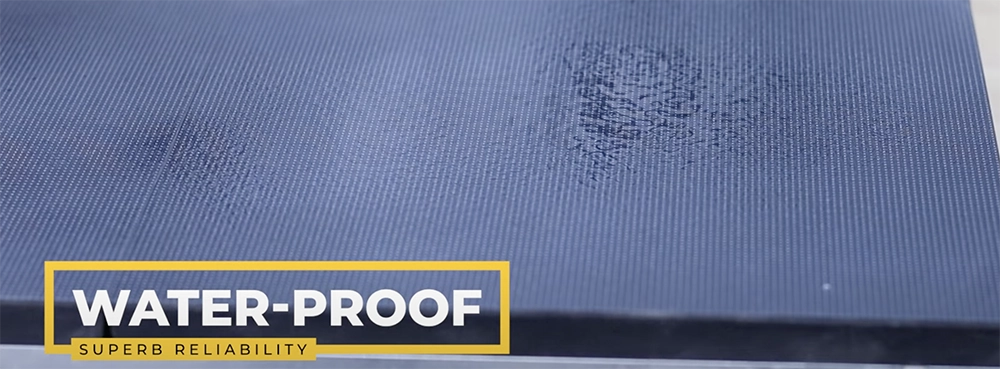
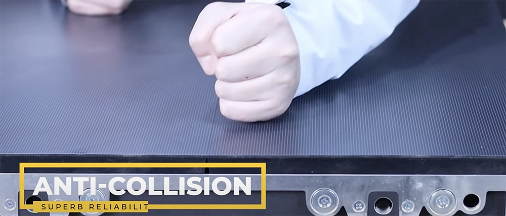
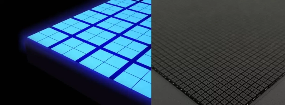
COB LED technology epitomizes innovation by directly mounting RGB LED chips onto a Printed Circuit Board (PCB) and encapsulating them with a protective layer. This approach enhances the durability of LED displays, making them more resistant to physical impacts and environmental elements. A notable advancement facilitated by COB technology is the achievement of finer pixel pitches below 1.0mm, thereby enabling high-resolution displays with improved visual comfort and reduced eye strain.
Advantages Over Traditional Technologies
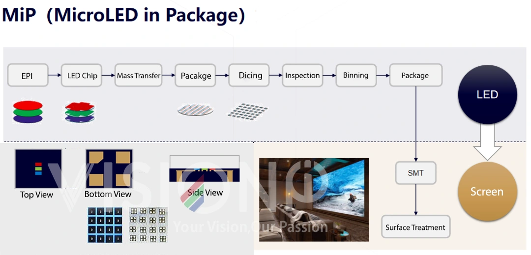
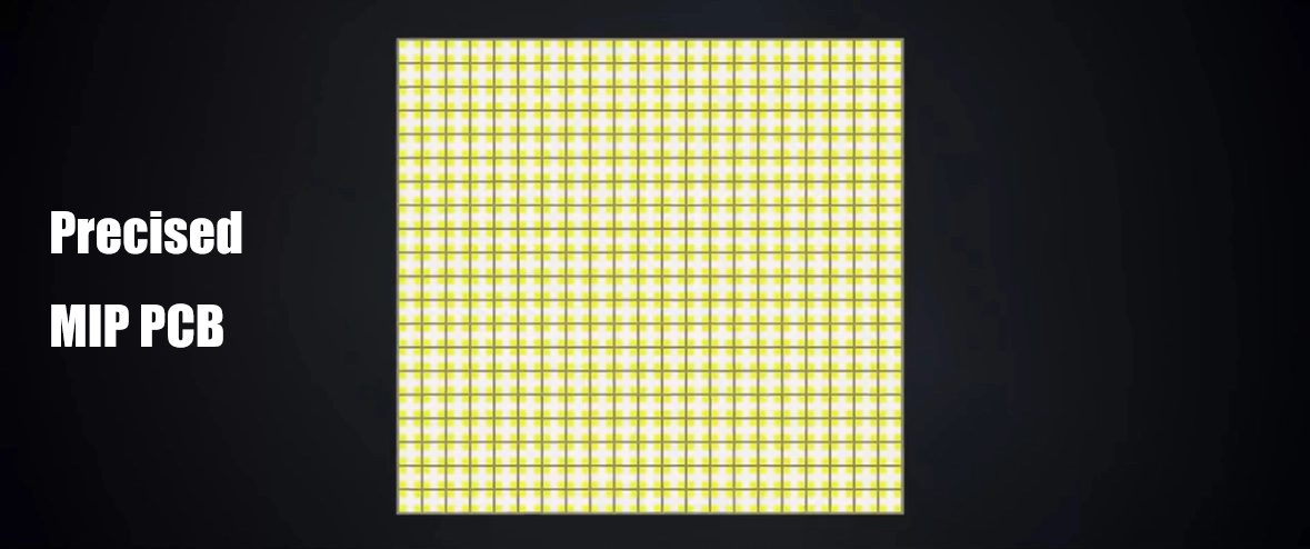
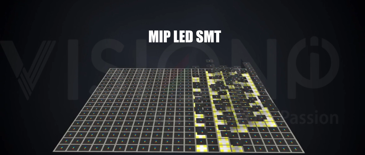
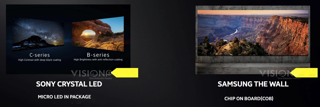
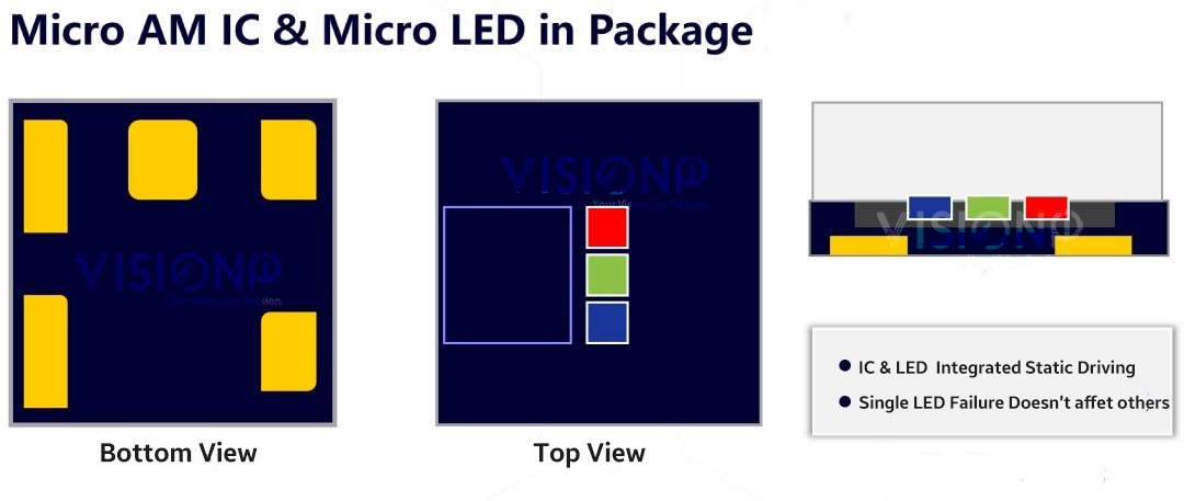
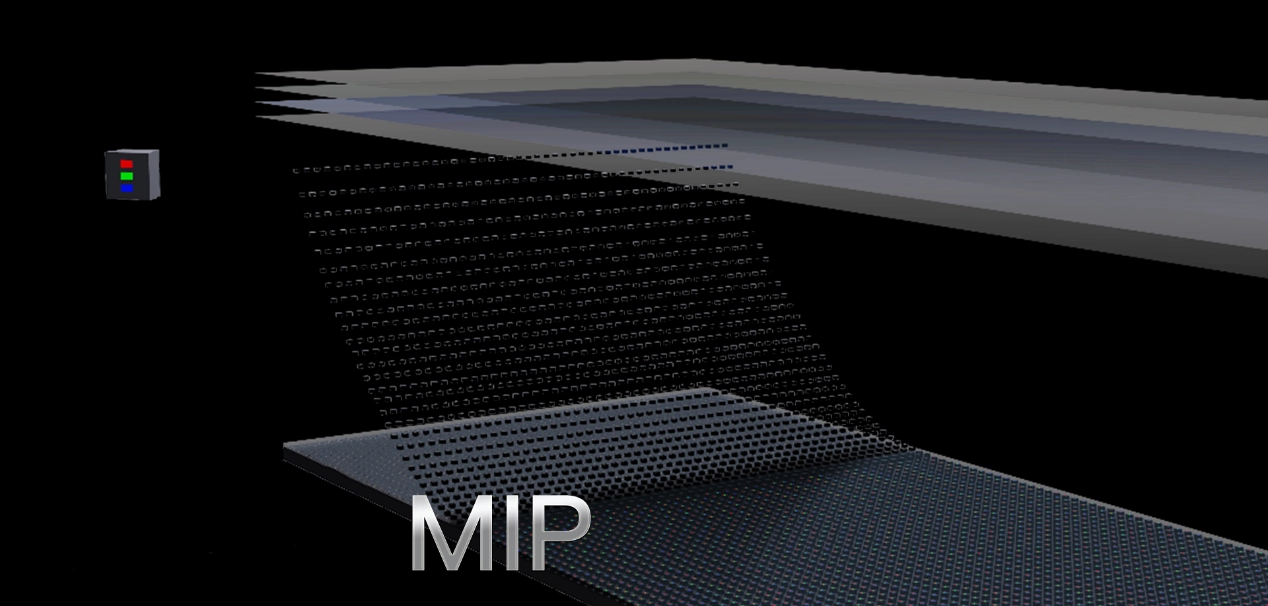
The transition towards COB technology reflects a response to the limitations faced by Surface Mounted Device (SMD) technology, especially as the demand for finer pixel pitches and higher resolutions grows. Unlike SMD and other competing technologies like IMD (Integrated Matrix Device) and MiP (Micro LED in Package), COB stands out for its superior pixel precision, robustness, and efficient heat management. These attributes contribute to its applicability across various sectors, including outdoor displays, which demand high durability and visual clarity.
COB LED Display Major Market Players
The Flip-chip COB LED Display sector is marked by intense competition, featuring a lineup of key companies battling for dominance. Leading the charge in this market are industry giants such as Samsung, LG, Sony. And some Chinese manufacturers :Hongli Zhihui Group Co., Ltd., LP Display, Shenzhen Visionpi Display Technology Co., Ltd., VMTC, Leyard Optoelectronic, CreateLED Electronics Co. Ltd., and Absen.
Samsung stands out as a pivotal force in this arena, recognized for its groundbreaking flip-chip COB LED display offerings and a robust global footprint. The brand’s market ascension is propelled by its dedication to research and development, alongside a continuous streak of product innovations. Samsung’s footprint in the flip-chip COB LED display domain is speculated to span several million dollars in market size.
Sony emerges as another formidable entity within the flip-chip COB LED display landscape. The brand’s reputation for delivering premium quality displays is complemented by its influential stance in the consumer electronics sector. Sony’s trajectory in this niche is powered by its commitment to enhancing visual experiences and versatility in application range. Its market presence in the flip-chip COB LED display sphere is also estimated to be several million dollars.
Leyard Optoelectronic, specializing in LED display solutions, showcases a robust lineup of flip-chip COB LED displays, contributing to its steady market progression. This growth is underpinned by a solid customer foundation and strategic alliances, positioning Leyard Optoelectronic’s market valuation within the flip-chip COB LED display sector at several million dollars.
While specific sales revenue details for these companies remain undisclosed, their significant roles in shaping the flip-chip COB LED display market are unmistakable. Entities like Samsung, Sony, and Leyard Optoelectronic have not only exhibited remarkable market evolution but are also poised for further expansion within this dynamic industry. The overall market valuation for flip-chip COB LED displays is projected to extend into several million dollars, with anticipations of continued advancement moving forward.
COB LED Display Solutions
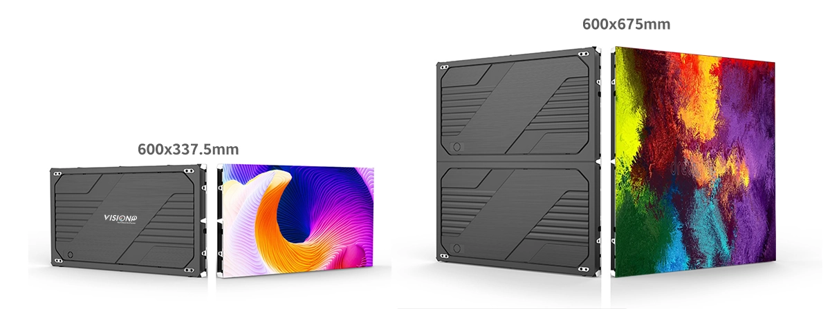
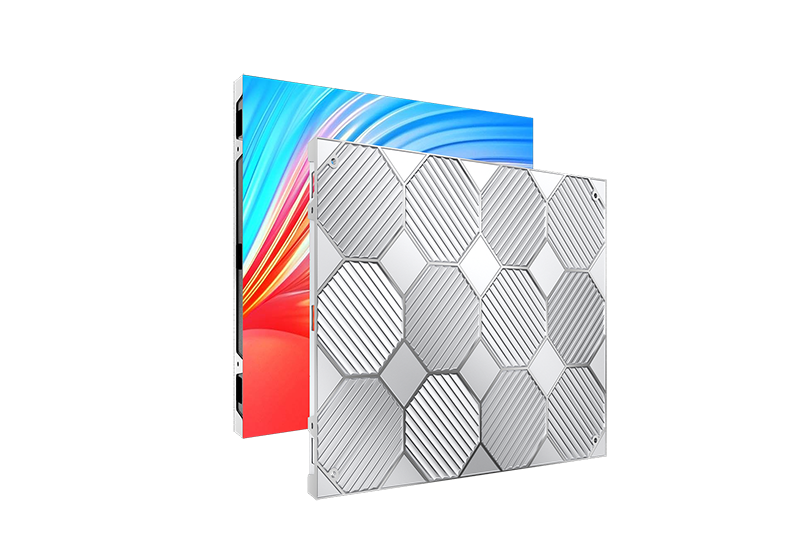
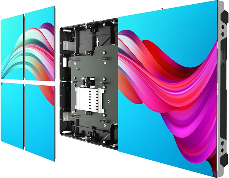
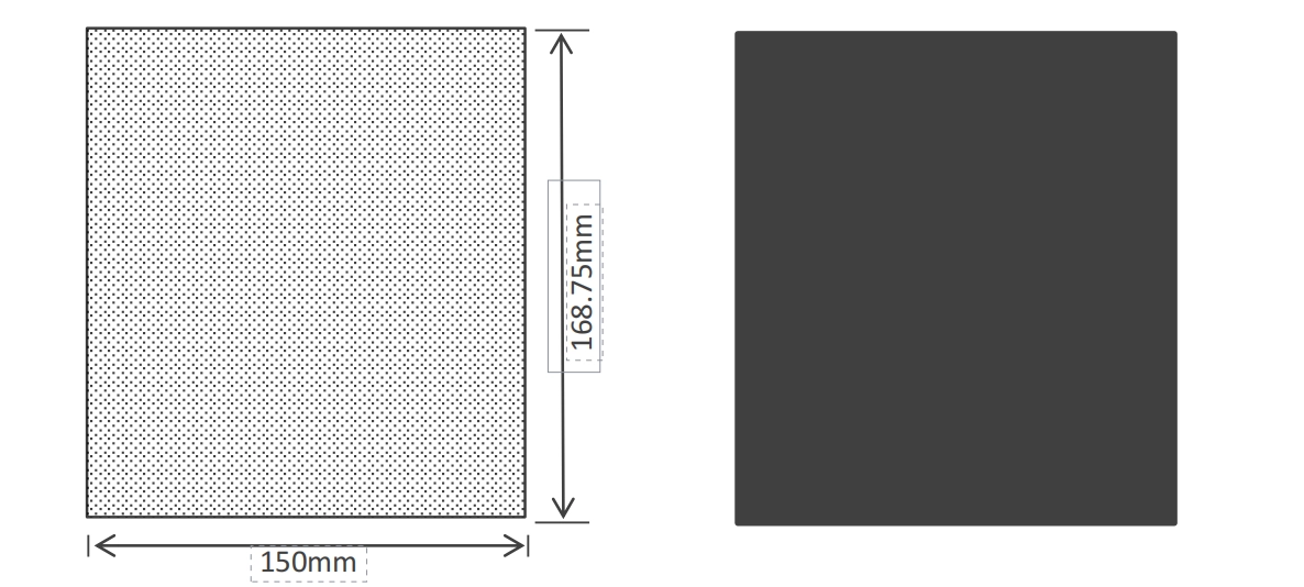
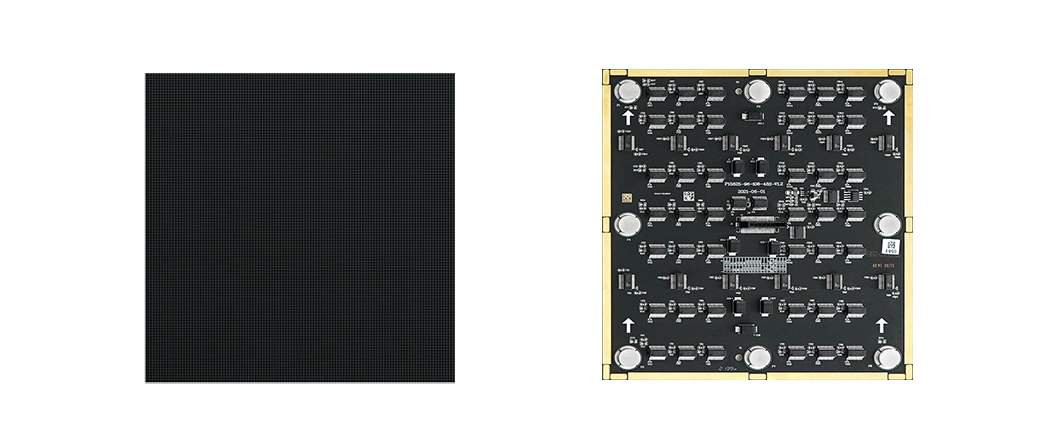
COB LED Display Modules/Tiles
Conclusion
As we look towards the future, COB LED technology continues to represent a promising path for the evolution of display technologies. Its superior attributes, coupled with the industry’s efforts towards cost reduction and technological refinement, are set to broaden its adoption. The advancements in 2024 are but a precursor to the transformative impact COB technology is expected to have on the LED display market, making it not just a part of the future but a defining force in shaping the next generation of display technologies.

