The Four Levels of Chinese LED Display factories

visionpi manufacturing
  • Level 1: the recently-created and unstructured workshop; and the factories only make the assembly work with all the half-completed product purchased from other suppliers, there are thousands of factories like this.
  • Level 2: the semi-organized factory that got out of level 1 but is still struggling to keep quality & timing under control, they have SMT machines, they can produce led panels themself, and focus on the segmented market, like led poster, rental display, transparent.
  • Level 3: the factory that made big efforts to get organized, with the objective of pleasing large customers, and they usually with many years of experience and their own R&D team and overseas sales team. here we can name a few, chip show, GCL, SBC.Yestech.
  • Level 4: that rare birds like Yaham, Unilumin that applies Lean manufacturing, and that avoids level 3’s rigidity.

In this article, I am excluding Chinese state-owned enterprises, which are a breed on their own.

Most manufacturers are at level 1 or level 2:The 4 levels of Chinese manufacturers

Level 1: the unstructured led display workshop

Typical profile:

  • 0-50 workers, engaged in simple processing (often assembly);
  • Managed by the owner and his family;
  • Not mature quality system and quality control staff;
  • No ability or time to work on complex prototypes before production starts;
  • Focused only on “making production” fast and on the cheap;
  • Can accept small orders, as long as purchasing components in small quantity is possible;
  • Seldom works directly for export customers;
  • Count on other manufacturers or trading companies to get business.

Result: low costs and low MOQs, but needs to be followed very closely by customers.

Level 2: the semi-organized led display manufacturer

This category is a mixed bag. Some export 100% of their output and are very familiar with their market’s quality & safety standards. Others focus more on the domestic market or the most price-sensitive countries (Middle East, India…), and should be avoided by importers from North America and Europe.

Still, it is possible to draw a somewhat typical profile:

  • 50-100 workers
  • Has grown out of the “disorganized workshop” stage
  • Has had to hire a few professional managers because of the growing complexity of operations
  • Has had to hire a few QC employees, to avoid big disasters.
  • But still, low concern for quality among staff and managers (in most cases).
  • May have English-speaking salespeople if direct relationships with foreign customers is a goal.
  • May still get orders mostly from trading companies and other factories.

Result: costs are relatively low, and quality & timing are relatively unstable. The owner’s motivation for your orders still determines their reliability.

Level 3: the organized/Listed led screen manufacturer

Typical profile: 200+ workers, usually established before 2010 with decade experience.

They have tried hard to comply with demanding buyers’ requirements:

  • Every aspect of production is specified in detail;
  • Production is checked thoroughly by QC department;
  • Own R&D team and updating led
  • Hopefully, strong staff discipline to follow the system;
  • a team for export business,and 60-80% of their sales is come from exporting.

Result: few quality issues, but high indirect labor costs (QC, middle management) and low flexibility. Top 10 led sign board manufacturers

Level 4: the continuously improving led display manufacturer

Typical profiles:

  • Part of a large multinational group or a joint venture.
  • Midsize factory with a process-oriented/engineering-oriented general manager.
  • dedicated to segment markets, like transparent led display or soft led display.

They follow the lean model:

  • Regular improvements to material flow and to each process;
  • Errors are prevented or corrected at the source;
  • Staff is trained and supports the philosophy.

Result: high customer satisfaction (close to zero defects; production cycle below 5 days) and relatively low cost (high productivity of operators, limited QC staff, and rework).

Unfortunately, these companies are a very small minority. They usually don’t advertise themselves on B2B directories. They are very hard to find.

What kind of Chinese factories should you work with?

First, a couple of rules to keep in mind:

  • If you work with a supplier that is too large relative to your orders (e.g. you would occupy 1% of their annual capacity), you will be quoted high prices and given poor service.
  • If you work with a small supplier that cannot produce the quantities you order, they will be forced to subcontract production and you will probably be in for a disaster.

My general advice would be as follows:

  • If your orders are very small, you might need to work with a trading company/quality assurance team that will place your orders in a level 1 factory and follow production.
  • If your orders are large enough to work directly with a manufacturer, but not big enough to be interesting to big factories, go for level 2, but you will still need a final inspection service before the shipment to make sure everything settled.
  • If your order is considered large and even big companies actively fight for your business, go for level 3.
  • If you are in a very quality-sensitive market and you cannot afford even 1% of defects, spend time and search for level 4 (but you might not find any in your vertical).

Small importers tend to have the feeling that buying from a large factory is more expensive but more reassuring. There is some truth regarding the higher prices, but risks are not necessarily lower. the fierce competition makes the industry more of chaos. after all, the company needs to survive, if the price allows them little profit, they will have to find a way to saving the cost from the raw material. smaller companies who dedicated one or few product line can be a good one to work with. 

We believe the core comptiveness is on the supply chain managment of a whole supply chain not between companies. VISIONPI dedicated in the supply chain management since the very beginning of the led display industry,back to 2000. we works with hundreds to thousand of importers to make the full adavantage of the supply chain in china.our professionla quality control team and managing system allow us to take the most advantage of the supply chain to provide our cusotmer with the best products.

What do you think?

LED display price increased? how ?

Since the beginning of the new year in 2021, major upstream raw material manufacturers in the LED display industry have successively issued price increase notices, leading to continuous increases in the purchase cost of LED raw materials (see details). As the upstream price increase surges all the way, the wildfire of price increase still burned to the downstream enterprises of the manufacturing, LED display companies such as Leyard, Unilumin, Absen have also issued price increase notices.

Leyard

On May 14, Leyard released the “Explanation on Global Price Increase of LED Display Products”. Leyard said that because of the increasingly tight supply of major upstream raw materials (semiconductor chips, lamp beads, PCB, etc.) and the significant increase in costs, Leyard, as the world’s largest LED display manufacturer, can still guarantee materials supply. but the increase has also led to a corresponding increase in the production and manufacturing costs of our LED display products.

To ensure R&D investment, product quality improvement and achieve this year’s production and operation goals, Leyard’s production bases will increase the ex-factory prices of products globally from May 17, 2021; it is expected to affect different series of Leyard products The market sales price of the country increased by 3-15%.

Unilumin

 It has to be said that the price increase of raw materials is a problem for the entire industry, and fierce competition makes it difficult to pass the cost completely to the end-user.

Hu Yan, Chief Financial Officer of Unilumin Technology Corporation, recently stated on the investor relations interactive platform that the price increase of upstream raw materials is a problem for the whole industry The company will balance the target value and adjust the price of some products appropriately to release part of the pressure.

Absen

Absen said that the company will adjust its sales price to customers based on market competition and company strategy.

In response to the increase in raw material prices, Absen stated at the investor interaction event on May 7 that the company adheres to the core values ​​of “integrity, gratitude, and responsibility”. uses its advantages to strengthen cooperation with upstream suppliers, and obtains strategic upstream suppliers. Support; At the same time, based on capacity forecasts and production planning, strategic stocking of key materials to ensure relatively low-cost material procurement and supply guarantee; In addition, the introduction of new materials, new technologies, and new equipment applications to improve efficiency and reduce overall cost.

 How much did the price go up?

Looking back at the origin, the price increase of various upstream raw materials, and the mismatch of various supporting devices and materials, have played a role in promoting the price increase of display products.

Previously, according to statistics from Experts, among the materials involved in display products, chips increased by 15-20%, driver ICs increased by 15-25%, metal materials increased by 30-40%, and PCB boards increased by 10- 20%, RGB devices increase by 4-8%, and display screens increase by 10-15%. (PS: As the price trend continues to rise, the price increase information may be lagging. Please refer to the latest announcements of the current companies.

How shoud we  deal with the price increase.

In my opinion, the current price is likely to be the lowest price for a long time in the future. Moreover, as long as the price goes up, it will be difficult to call back, because it is impossible to take back the US dollars issued by USA and the currency issued by other countries.

In addition, the major shipping companies have also joint to raised prices recently, I hope you can make reasonable order & shipping plans.

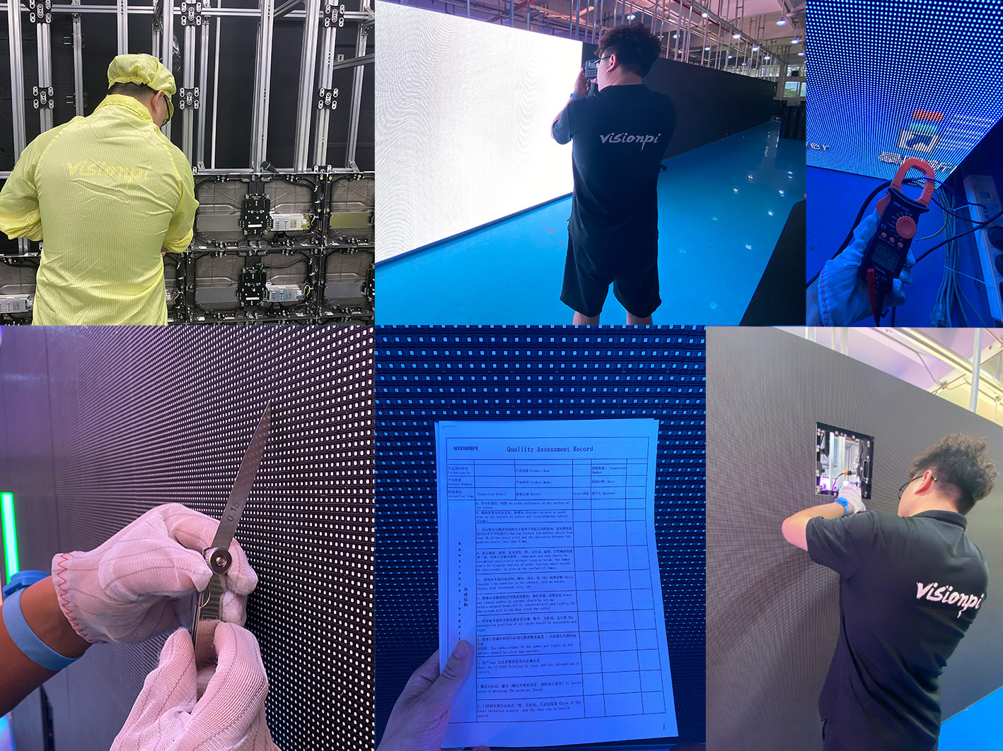
LED Display Quality Inspection Checklists

LED Display quality control

led display inspection

Understand the LED Display Production Process

Step 1: Technical study

An exclusive professional department with more than a decade of experience in advertising LED screen manufacturing will thoroughly study your needs and the technical concepts required for a new order.

Step 2: Structural design

We will design the frames of a big LED screen to adapt to the features and sizes requested by you perfectly.

Step 3: Assembling of structural components

We will assemble the manufactured structure in such a way that there is no visual separation in the whole unit. All the inside pieces will be placed according to a pattern and perfectly aligned by laser.

Step 4: Electronic components

We will program the assembling of electronic and LED equipment to assure that only the parts corresponding to your order are used. This is one of the most complex and delicate tasks of the entire process. It is the most important phase of creating the LED advertising screen.

Step 5: Assembly of electronic components

We will assemble the circuits we manufacture to create complete panels, which are fully functional and capable of reproducing a full-color image.

Step 6: Tuning and adjustment

We will adjust the LED panels to light and chromatic levels to ensure that sharpness and color are the same in the entire LED advertising screen. To do this, we will use photoelectric sensors measuring chromatic patterns adjusting and memorizing each LED component.

Step 7: General assembly

We will assemble the structural frames and parts to form complete units capable of reproducing videos.

Step 8: Assembly test

We will activate the screen as a whole and carry out exhaustive testing. Once all the tests prove smooth functioning, we will proceed to the image management and control phase.

Step 9: Image test

We will reproduce several test videos during the image control phase. We will analyze the chromaticism and its quality level. Finally, we will tune everything to adjust the whole unit.

Step 10: High protection packaging

We will carefully pack the LED screen into a high-resistance package to ensure product protection during transportation.

LED Display Quality inspection Details

Quality control of LED display is a process of ensuring that the LED display screen meets the desired standards of performance, reliability, and color accuracy. There are several aspects of quality control of LED display, such as:

  • Defective pixels: Defective pixels are pixels that do not function properly or do not emit light at all. They can affect the overall appearance and quality of the LED display.
  • Uniformity: Uniformity refers to the consistency of brightness and color across the LED display. A good LED display should have uniform brightness and color without any noticeable variations or spots.
  • Color accuracy: Color accuracy refers to the ability of the LED display to reproduce the colors of the original content faithfully and realistically. A good LED display should have high color accuracy without any color distortion or deviation. To test for color accuracy, you can use some online tools such as [DisplayCAL], which is a graphical user interface for the display calibration and profiling tools of Argyll CMS, an open source color management system. You can also use a colorimeter or a spectrophotometer to measure the color gamut and color temperature of your LED display.
  • Sharpness: Sharpness refers to the clarity and detail of the images displayed on the LED display. A good LED display should have high sharpness without any blurriness or pixelation. To test for sharpness, you can use some online tools such as [Lagom LCD test], which is a series of test images that help you to adjust the settings of your monitor. You can also use some test patterns or images that have fine details and edges to check the sharpness of your LED display.
  • Viewing angle: Viewing angle refers to the angle at which the LED display can be viewed without losing image quality or color fidelity. A good LED display should have a wide viewing angle without any color shift or contrast loss. To test for viewing angle, you can use some online tools such as [Viewing Angle Test], which shows you how the colors and contrast change when you view your monitor from different angles. You can also use some reference images or videos that have various colors and contrast levels to check the viewing angle of your LED display.

quality led

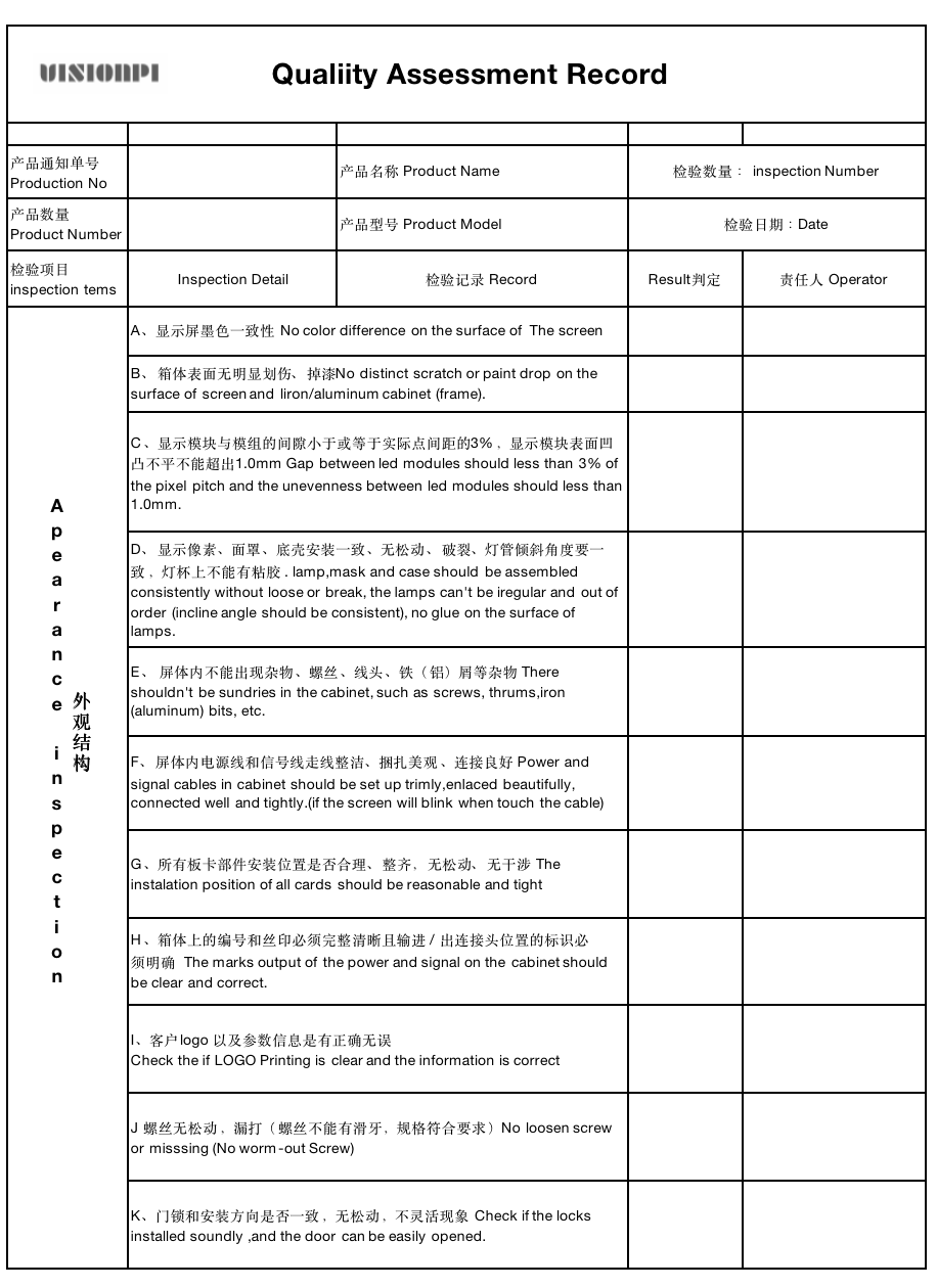
Example of inspection checklists

A good checklist is central to managing quality

Managing quality is a bit like coaching a professional sports team. A big part of the job is about repeating the same thing over and over, to get the basics right.

If you buy a led display from a supplier located thousands of miles away and rooted in a different culture, There should be an order confirmation letter to the customer to check and sign back before arrange the productionyou really need to focus on the basics:

  1. Document your requirements.
  2. Make your requirements s specific and testable, so that they are ready to be used as an inspection checklist.
  3. Ensure your supplier, and especially the people who really count (their purchaser, their manufacturing staff, their quality staff), is aware of your requirements and commits to hitting them.
  4. Inspect products based on your checklist, and request rework/reproduction if needed..

How to organize a QC inspection checklist

First, you have to think of the best way to guide an inspector through the job. For LED DISPLAY inspection checklist, it generally involves:

  • LED Brand (verification, the resources, and the batch number) copper wire or golden.
  • Driving IC (Brand and model)
  • Power supply and receiving card
  • cables (pure copper)
  • special functions: calibration or high temperature resistant
  • performance( viewing angle, error rate,uniformity of color )
  • Appearance check
  • Package
  • Reliability testing

Then, at each stage, you need to think about what details to check. and what standard?

  • Were specific requirements given to the supplier? Go through those requirements that are really important.
  • Any safety or regulatory considerations? Definitely cover them.
  • Are aesthetics important? Define what to look at and what common issues are to be counted as defects.
  • Any function test, endurance tests, or any similar?

Once you know what needs to be checked, the most important questions are:

  • How to check this criterion, and what will consider a pass or a fail?
  • How many samples should I check for this point? (Some checkpoints take a long time and/or destroy samples, so smaller sampling sizes may make sense.)
  • What measuring/testing equipment will be necessary? Will the inspector bring it, or will the factory have to provide it?

LED Display Quality inspection service

VISIONPI QC is a Sino-foreign joint venture quality assurance, project management, and product engineering agency based in China. We are dedicated in A&V products for decades and our key focus is on transparency and control in your supply chain. We offer startups and SMEs the expert assistance you need on the ground in China to improve your relationship with, management of, and quality from your Chinese supply chain,We never hold any of your information for ourselves to ‘lock you in’ We work exclusively for you, and we share and investigate all the information we have in or out of our database for you.

led display inspection service

Are microLEDs the next big thing for display technology?

Are microLEDs the next big thing for display technology?

Are microLEDs the next big thing for display technology?

Sized to be individual display pixels, microLEDs are under heavy development, with emphasis on singulating, packaging, and assembling these LEDs into displays.

What is a microLED?

The term microLED typically refers to the size of the emitting area of the LED device. However, there is no clear industry clarity on the size that qualifies as “micro”—and the definition can vary based on the application. For example, for virtual-reality and augmented-reality(AV/VR) glasses, the desire is to have microLED elements that are smaller than 10 μm. For direct-view displays, some like the definition to be 50 or 100 μm. Above this size is a new category called miniLED; again, no clear emitter size range has been agreed to.

To make things even more confusing, many display companies are simply calling their latest very-fine-pitch display pixels “microLEDs” regardless of the size of the emitter being used. This is because for a display device, it is the pixel pitch (the space between full-color pixels) that is more important than the LED emitter size.

The most-familiar type of direct-view LED (DV-LED) display is a so-called “videowall.” These are modular displays made from a number of “cabinets,” with each cabinet composed of several “modules.” Each module in turn has red, green, and blue(RGB)LEDs mounted on a circuit substrate along with drivers and electrical interconnections.

Over the last few years, there has been a clear trend toward narrow- or fine-pitch LED video walls. These are generally defined as pixel pitches of under 1.5 mm, with the latest prototypes now at 0.4 mm. Such displays are designed for closer viewing distances. For perspective, 0.4 mm is very close to the pixel pitch on a 65 in. 4K-UHD resolution TV. As a result, major TV brands are very interested in this technology.

DV-LED displays can meet and often exceed LCD or OLED performance in terms of luminance, dynamic range, color gamut, viewing angle, black levels, and so on. The main disadvantage is price. One of the main cost drivers for DV-LED displays are the RGB LEDs. Moving to smaller LED emitters mean less LED device material is needed—a substantial cost reduction. The other major cost factor is the packaging of the LEDs and assembly onto the module circuit boards.

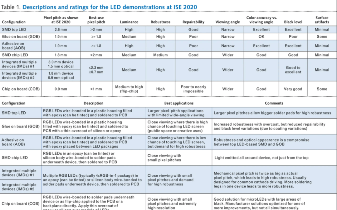
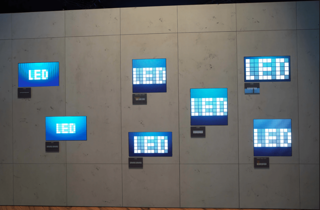
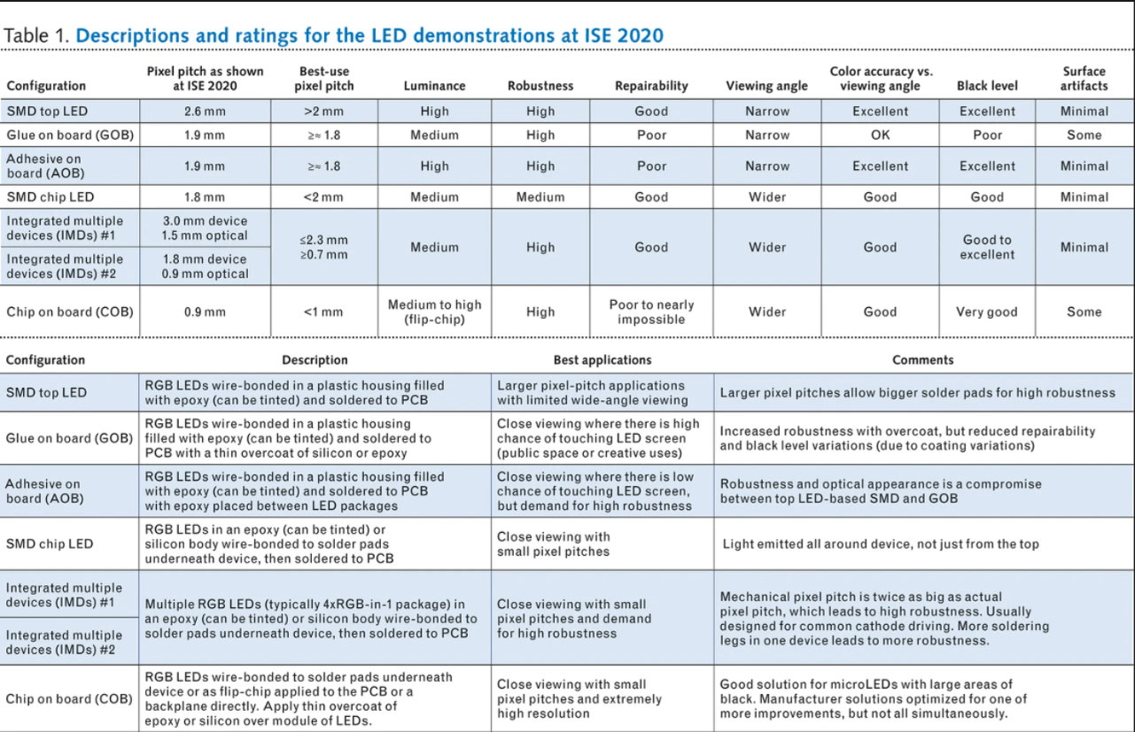
Historically, LEDs are diced from the epitaxial wafer, placed in a surface-mount package, wire-bonded in place, and encapsulated with epoxy or silicon (so-called SMD top LED). Variations in the way these LEDs are assembled on the printed circuit board (PCB) can be described as glue on board (GOB) and adhesive on board (AOB). Several newer approaches seek to reduce costs and allow smaller pixel pitches. These can be described as SMD chip LED, integrated matrix devices (IMDs), and chip on board (COB). A photo of the small-scale demo along with a table describing the configurations and strengths/weaknesses of each are shown as below:

However, it is likely that they are in the range of 100 to 300 μm in length or diameter, so either microLED or miniLED, depending on the microLED definition.

At ISE, Visionpi (Shenzhen, China) showed a state-of-the-art 0.4-mm-pitch DV-LED microLED video wall. This is a flip-chip COB approach probably to a PCB backplane. This prototype is a single-chip solution.

COB FLIP CHIP LED WALL webp

Note that the distance between each RGB set of LEDs is 0.4 mm, so the active LED diameter is around 70 μm, which is below the 100 μm microLED threshold that some use as a definition. Also note that as the active LED area gets smaller, the surrounding black area gets larger. This creates a display with a better black level and higher contrast. Sony’s Crystal LED video wall has a pixel pitch of 1.2 mm with emitters that are thought to be about 100 × 35 μm in size, leading to a display with 99% of the area being black with really great performance.

Visionpi is a company that offers display solutions to its mainly rental and staging customers. Their showcase at ISE was designed to help illustrate the difference in image quality one gets with these different packaging and manufacturing approaches. Visionpi uses a single flip-chip approach overcoated with a thin layer of adhesive silicon and black adhesive between the flip-chip devices. This display uses microLEDs with a pixel pitch of 0.83 mm and has a luminance of 2000 nits.

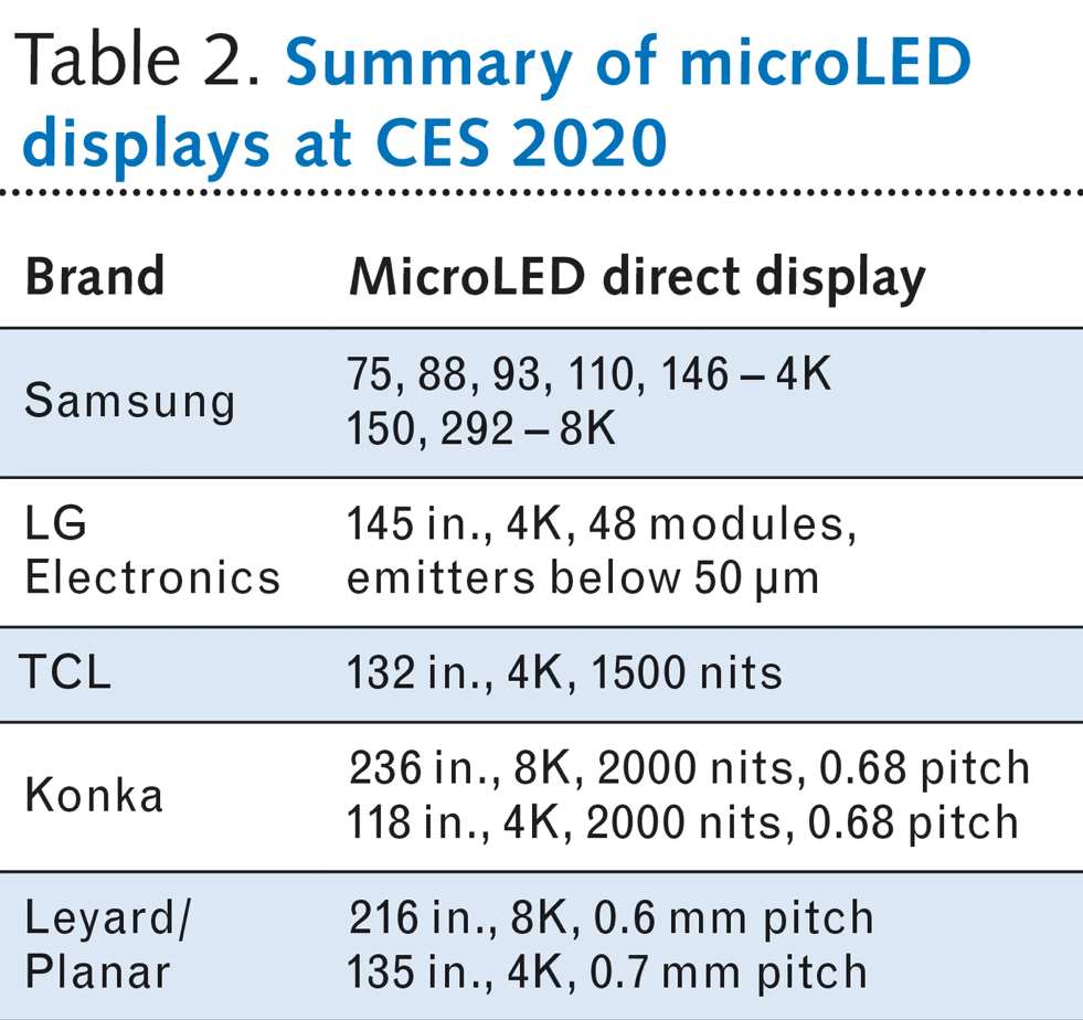
TV brands are also very interested in microLED technology. At CES 2020 (January 7-10; Las Vegas, NV), Samsung expanded its line of microLED-based displays called “The Wall,” while others exhibited various prototypes that they hope to bring to market in 2020 (see Table 2).

Challenges remain for all these technologies, which impacts their high costs. For example, most DV-LED displays still wire-bond the LED inside the package or to the PCB. Flip-chip devices eliminate all the wire bonding, but require that the surface of the LED epiwafer be planarized so the n and p contacts are at the same level. The device can then be flipped over to directly solder to the PCB.

Wire-bonded multi-in-one IMD devices are available today, as are single flip-chip LEDs, but they are not yet very common. IMD flip-chip devices are still only available as prototypes.

Singulating the individual die or IMD devices also has its issues, too. When a laser is used to separate the die, it can leave rough edges that reduce the black level. Overcoats of epoxy can also have thickness variations leading to variations in black level over the display. In addition, bad LEDs need to be removed and replaced in the manufacturing process, which can vary from doable to nearly impossible.

As Lucas. W, Director of LED & Displays at visionpi, noted, “Each LED videowall supplier working on COB has some unique processes to optimize cost and performance parameters. The reality is that some have optimized one set of parameters and another a different set, but none have optimized all just yet. However, the fact that most of them can be solved already makes us confident for the future of COB.”

Developing next-generation microLED manufacturing

One fundamental issue with DV-LED displays is that the LED pitch on the epiwafer is very small, while the pitch on the DV-LED display can vary widely. Current mass transfer methods can transfer one to dozens of LED chips at once. To truly become cost-competitive with LCD or OLED displays, the transfer rate must increase to millions per minute. As a result, this is where a lot of innovation is concentrated now.

The most-common approach is a stamp transfer that can pick up thousands of microLEDs at a time and transfer them to a separate substrate with a different pixel pitch. Another approach uses laser pulses to transfer LEDs from a carrier substrate to the display substrate. Few details about these and other approaches are ever revealed, as they are considered proprietary intellectual property.

The next problem to worry about is yield. Not only must the mass transfer be extremely fast, but placement must be very accurate. As the size of the microLED gets smaller and smaller, the ability to pick up and accurately place it becomes more and more difficult. If a defect is found, is there a repair process that does not take far longer to complete than the initial mass transfer time? And this just applies to mechanical/electrical yield.

All the LEDs must also fall within a certain range of luminance and wavelength to provide the kind of performance demanded by end users. This is pushing the LED wafer makers to improve the way the LEDs are fabricated. New MOCVD chambers with much better uniformity and layer control are now available to enable most of the wafer to fall within quality control guidelines. Traditional gallium nitride (GaN)-based blue and green LEDs are grown on sapphire epiwafers with a 2 to 6 in. substrate size. To lower costs, larger wafer sizes are desirable. Consequently, GaN-on-silicon epiwafers are also being used to grow green and blue microLEDs at 8 in. sizes now, with the potential to go to 12 in. wafers later.

Many of these requirements point to the need to have a way to fully characterize the microLEDs at the wafer level prior to any mass transfer method. Companies are working on this need as well.

All these LEDs also need to be driven with signal to create an image. DV-LEDs mount the LEDs on a PCB and use a lot of driver chips to send signals, and next-generation DV-LEDs may well be mounted on glass substrates with active-matrix driving using TFTs at each pixel location. This will provide better control of each microLED and can leverage the TFT-on-glass fabrication infrastructure already in place for LCD displays.

Finally, since the display needs RGB LEDs, all the above improvements and techniques must be done three times for the RGB wafers.

Subscribe To Our Newsletter

Join our mailing list to receive the latest news and updates from our team.

You have Successfully Subscribed!

Pin It on Pinterest