LED display packaging has developed from early-days DIP (dual in-line package) to today’s multiple packaging methods such as SMD, IMD, and COB,. These methods have reshaped the industry.
COB technology eliminates the process flow of SMD light-emitting tube packaging, color separation, taping, and patching, simplifies and improves the reliability of the product production process. Longer Life Span: Without the holder, the LED chip has lower heat resistance, largely increasing its life span
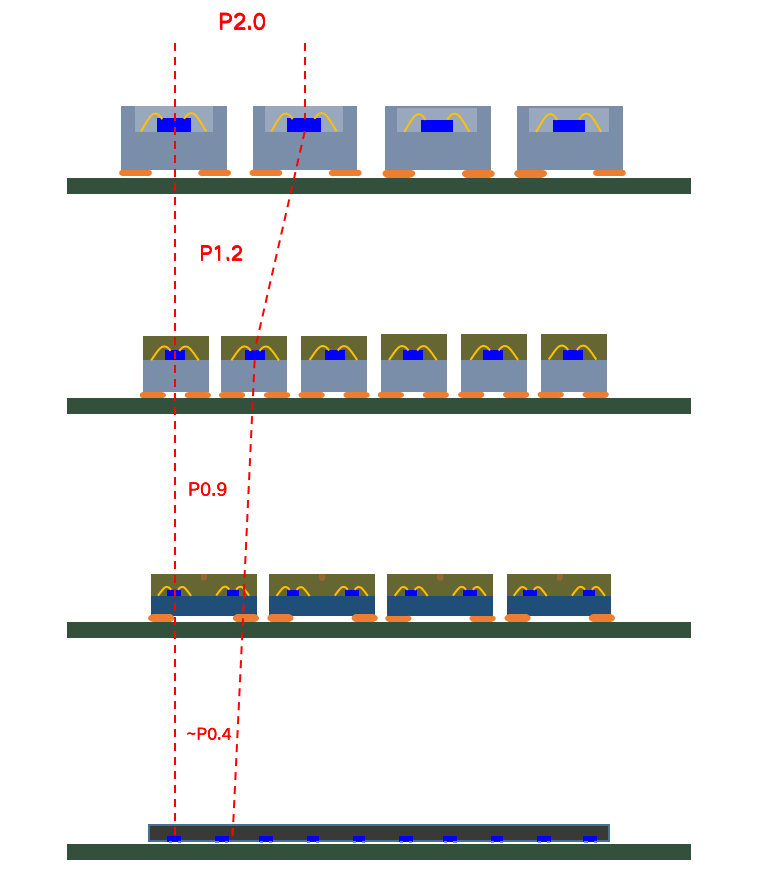
Smaller Pixel Pitch: the pitch of SMD is P1.2-P2.0, while COB is P 0.5-P2.0 .The COB technology is not limited by the physical size, bracket, and lead of the SMD LED package, and can break through the SMD pitch limit, achieve higher pixel density, and have a more flexible dot pitch design.
COB more likes the surface light source than the SMD, when light refracts, it has less light loss. COB Realizes The Conversion From “Point” Light Source To “Surface” Light Source.No pixel graininess; can effectively control the brightness of the pixel center, reduce the intensity of light radiation, inhibit moiré, glare, and glare to the retina, suitable for close and long-term viewing, not easy to cause visual fatigue, suitable for close-screen viewing.
The PCB circuit board, crystal particles, solder feet, and leads are fully sealed. The advantages of the sealed structure are an obvious-for examples, moisture resistance, anti-collision, prevention of pollution damage, and easier cleaning of the device surface.
Wire Bonding COB. In wire bonding COB Also called (face-up cob or Lateral COB), the LED chips are attached directly to the substrate using an adhesive, and their electrical connections are made with thin wire leads. This method is quite traditional and widely used due to its cost-effectiveness and simplicity in connecting the LED chips to the driving electronics.
Flip chip COB, on the other hand, involves mounting the LED chip upside down on the substrate so that the light emits from the top, making direct contact with the substrate. This setup enhances heat dissipation, reduces the thermal path, and generally provides better luminous efficiency and reliability.

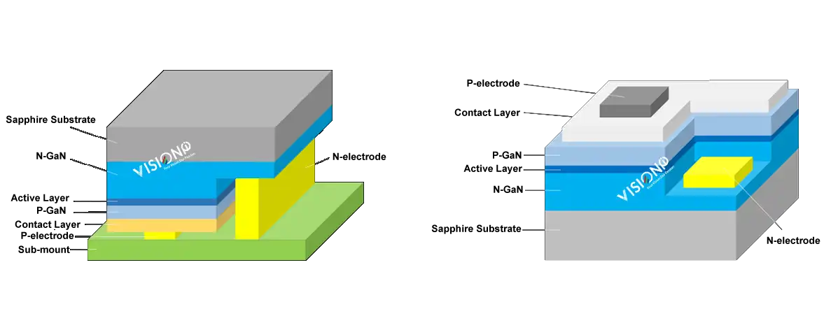
1. Higher stability. Flip chip packaging technology eliminates wire bonding, eliminating the risk of gold wire breakage and simplifying the production process.

2. Smaller pixel pitch. Flip-Chip COB encapsulation is the chip-level integrated encapsulation. Without the wire bonding, the physical space size is only limited by the size of the light-emitting chip, which can achieve higher pixel density.
3. Better visual performance. Regarding display performance, the area of the Flip-Chip is smaller on the PCB board, and the duty cycle of the substrate is increased. It has a larger light-emitting area, which can present a darker black field, higher brightness, and higher contrast Presenting HDR-level display effects.
4. Cost-effective. There is no welding wire link, simplifying the production process and reducing equipment investment costs. As the industry scales, the product cost will be significantly reduced, especially when the dot pitch is less than 1.0mm.
Therefore, Flip-Chip COB technology is a necessary condition for the realization of MicroLED and will go further in the era of micro-display.
The Future Of direct view led display.
Flip-chip COB is an upgraded version of lateral COB, flip-chip COB improves reliability and visual performance, simplifies the production process, and narrows the pixel pitch. COB is the future of direct view led display
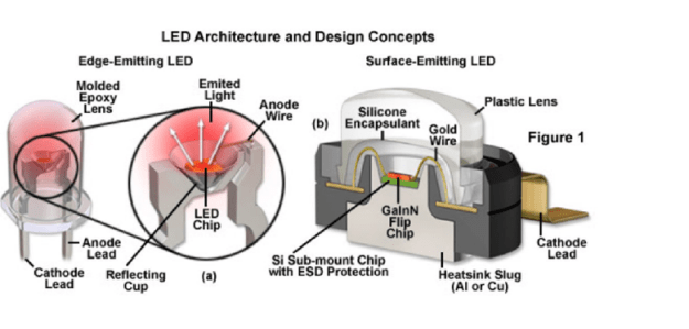
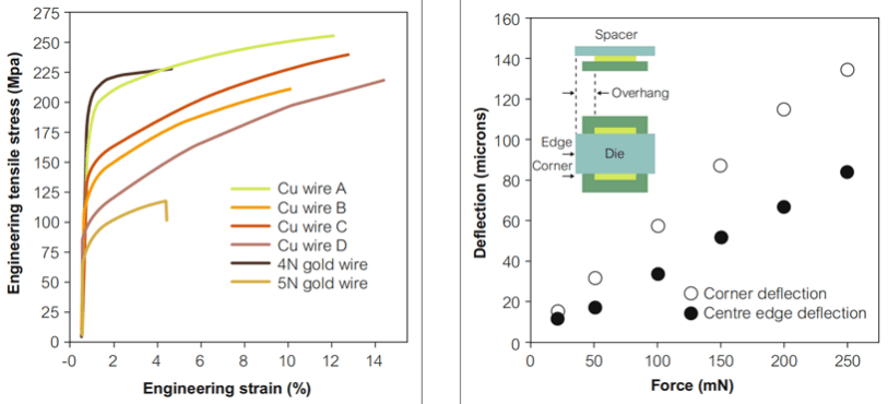
The conductor and wire bonding in the package is the apparatus that transfers electric current from the circuit board to the diodes. Conductors are located on the underneath or back side of the package carrier and consist of an anode and cathode division (positively and negatively charged). These pieces are manufactured from one of three different metals – Gold, Copper, silver, or even Iron. Copper Wire bonding refers to the wire bonding process that employs copper wires for interconnection, instead of the gold and aluminum wires traditionally used in semiconductor packaging.
There are variances in both conductivity and environmental performance with these three metals.
Gold is the preferred metal for both situations, having both the best conductivity and being the most environmentally resistant – but as expected it is also the most expensive.
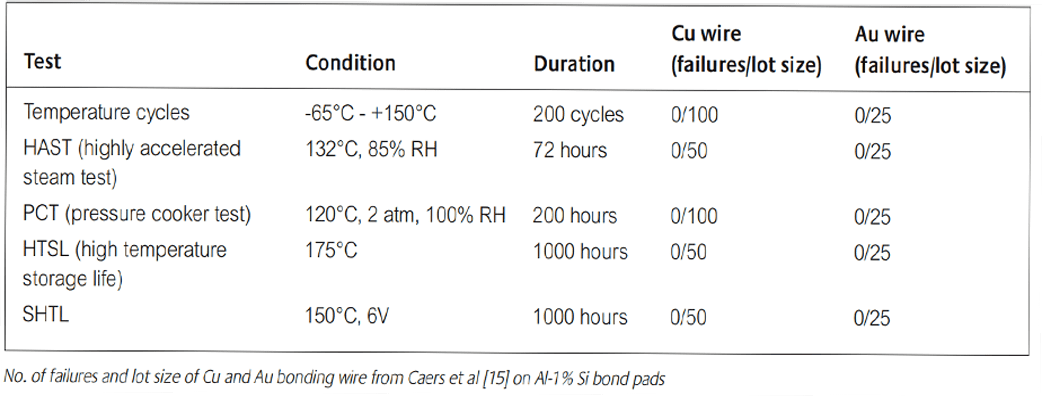
Silver/ Iron is the most susceptible to corrosion and Copper is not gold and it is unreasonable, given the different physical and chemical characteristics of each metal, to expect copper simply to bond in the same way as gold. From a performance point of view, copper can be as reliable as gold wire but copper is facing problems in more challenging stress tests such as temperature cycling, If you are in an indoor environment naturally this isn’t usually a concern with controlled, low-humidity.
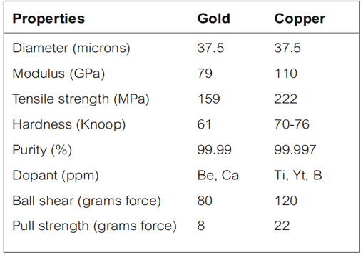
For this moment, gold wire still is the more stable one for the LED display. While larger-diameter copper wire has been utilized in many applications for some considerable time, the copper bonding wire is not a ‘drop-in’ solution for gold wire and should not be seen as such in fine and ultra-fine pitch applications. Copper wire from different suppliers can differ considerably in purity and mechanical properties during the process. That is why, for small pixel pitch, normally Gold wire is adapted.
Copper VS Gold Copper Wire bonding refers to the wire bonding process that employs copper wires for interconnection, instead of the gold and aluminum wires traditionally used in semiconductor packaging. Copper is rapidly gaining a foothold as an interconnection material in semiconductor packaging because of its obvious advantages over gold. These advantages include:
A. ReeStar ™ (“RS”), a high-end full-color display device launched in 2013, mainly has four models, is a high-end brand of indoor foreign star high quality LED screen, more than three years warranty, excellent performance can fully realize the led high-definition display, high contrast ratio, high waterproof, high reliability, low light decay and other requirements. requirements.
B. 7 Major Performance Advantages of RS
• a). Waterproof and moisture-proof: waterproof performance reaches IPX8 level; moisture-proof performance reaches MSL 2a level.
• b). Cold and thermal shock resistance: high bonding of packaging materials, -65℃~+150℃ cold and thermal shock without dead light.
• c). Anti-back pressure: meet the high refresh frequency demand, 85 ℃, 85% RH, simulated back pressure test without failure.
• d). Salt spray resistance: the use of a wide range of simulated seaside corrosive environment without dead lights.
• e). UV resistance: UV experiments accelerated aging outdoor simulation using 3 years, light decay is less than 20%.
• f). Low light decay: high temperature and high humidity accelerated aging simulation of outdoor use for 3 years, light decay <20%.
• g). High brightness: the highest brightness level in the industry.
C. RS’s 3 Major Appearance Advantages
• a). Matte surface, high contrast.
• b). Surface luminescence technology: turn point into surface, solve the problem of led glare.
• c). Low pin technology: high cup and short foot, easy for customers to fill glue and cover mask.
D. There Are 4 Main Models
RS-1921MBAR, RS-2020MBAM, RS-2727MWAS, RS-3535MWAR

Copper is inherently 2 to 5 times cheaper than gold, so substituting gold wires with copper wires can realize tremendous annual cost savings for a semiconductor packaging company:
let’s do simple math, you will see how much difference in price among those LED of varied bonding material: For example: P10, 10,000 Pixels/sqm with Nationstar LED 3535: Gold wire: High brightness: 20USD/K Copper Wire: Normal brightness: 10 USD/K Iron Wire: 5USD/K So Basically you can see the price difference, gold wire is about twice of copper. When it comes to indoor LED with a smaller pixel, the price can be a huge difference. if you see P2 (250,000 pixels/sqm),nationstar gold wire 1010 is roughly 8 USD/K.while copper wire is 4 USD/K. so it is about 1000 USD more. Most of the time factories /salespeople won’t tell you about the wire bonding material, unless you ask, even you ask, they can lie, because this no way you can recognize the difference by your eyes. except for chemical lab testing. Visionpi has a long term partnership with Nationstar/Kinglight, we provide verification service to our customers.
copper and gold wire bonding are both widely used techniques for connecting LED chips to external circuits in the LED video display industry. Copper and gold wire bonding have distinct advantages and disadvantages based on their intended use. Copper wire bonding is an economical choice that offers high thermal conductivity but has limited lifespan and low electrical conductivity. On the other hand, gold wire bonding, which is more expensive, provides thin wires and high electrical conductivity while having low thermal conductivity. Ultimately, selecting between copper and gold wire bonding should be based on the specific needs and requirements of your LED video display project.
Accurate information is the key to evaluating the quality and performance of any manufacturer’s LED DISPLAY. However, there are some manufacturers, who produce and sell LED MODULES in a large quantity, and they usually sell to other LED factories/companies.they are using mainly are iron wire bonding led (Mulinseng, HongSeng), for price sake. The competition is getting fiercer, there are small companies who sell inferior quality LED but claim to be a good one. Even now you know those brands and quality level. but you are unable to tell if it is real. After a few months running, the display will bleed you on the maintenance cost. Visionpi provides LED verification services, we can be your professional QC team to help you with the sourcing and inspection and bring lower purchase cost and guaranteed quality.check more our services.
The bare IC is mounted directly on the substrate on the back of the PCB, then using a special method of welding using a pure gold wire, a bond is made between the base and silicon chip, then finally the COB is packaged together to form the full-color module.
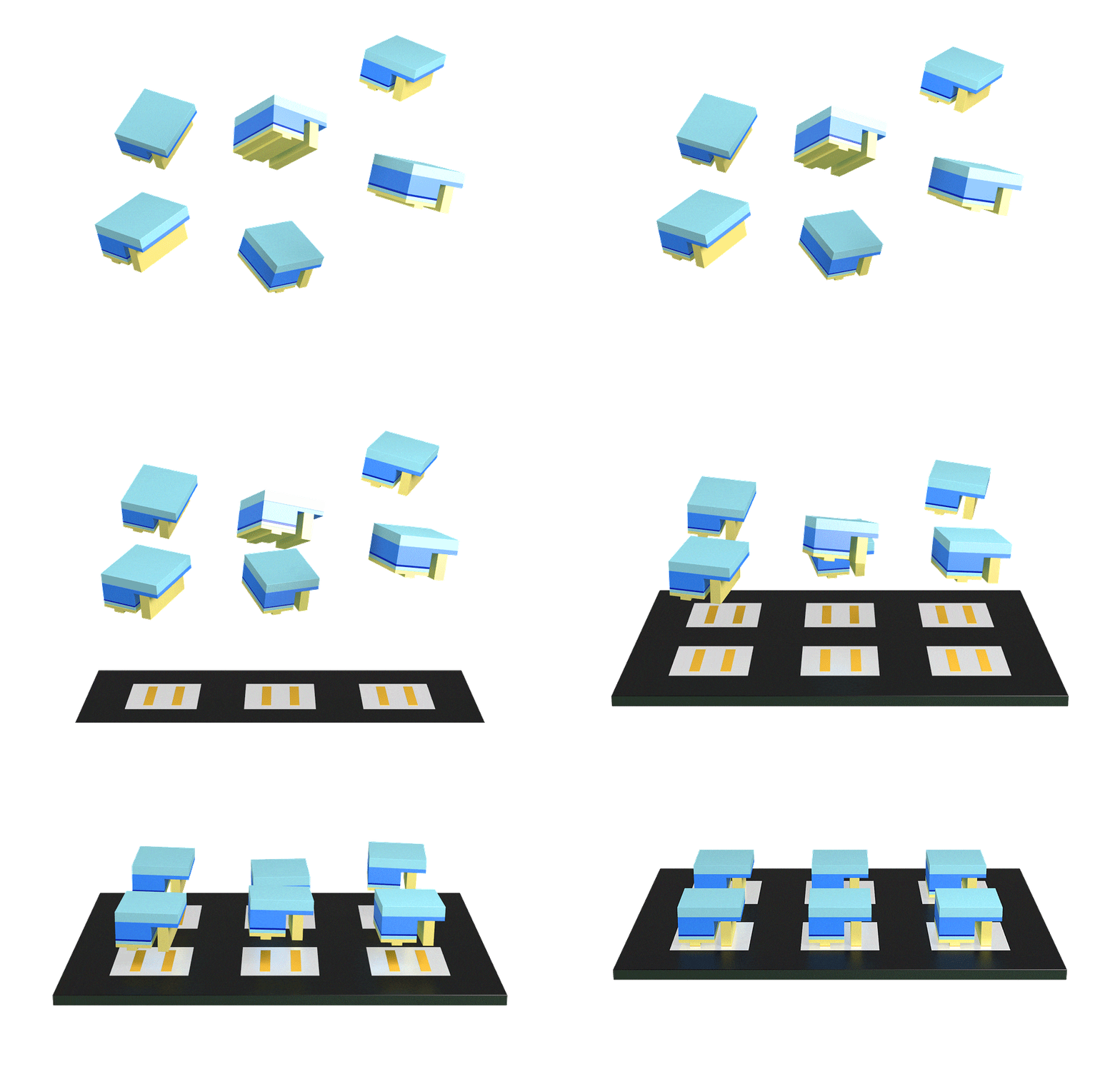
Micro-led Mass Transfer Technology
Mass transfer is a technique that can move Micro-LED chips from wafers to display panels.
This is the most challenging part of making MicroLED displays. There are three main challenges in this step “ accuracy, speed, and reliability.
The transfer process requires high accuracy, as each microLED chip is minuscule and has to align precisely with its designated location. The tolerance for deviation is very low.
The transfer process also requires high speed, as contemporary displays have very high resolutions. For instance, a 4K display comprises more than 24 million subpixels. To achieve cost-effectiveness and productivity, the transfer process has to handle multiple microLED chips simultaneously.
The transfer process also requires high reliability, as the display industry expects high standards and low defects. As the displays become larger and finer, the quality becomes more critical. We will elaborate on the microLED quality issue in a subsequent section.
Flip Chip COB series micro & mini LED display provides three types of surface treatments, including Brilliant Black, Natural Black, and Matte Black.
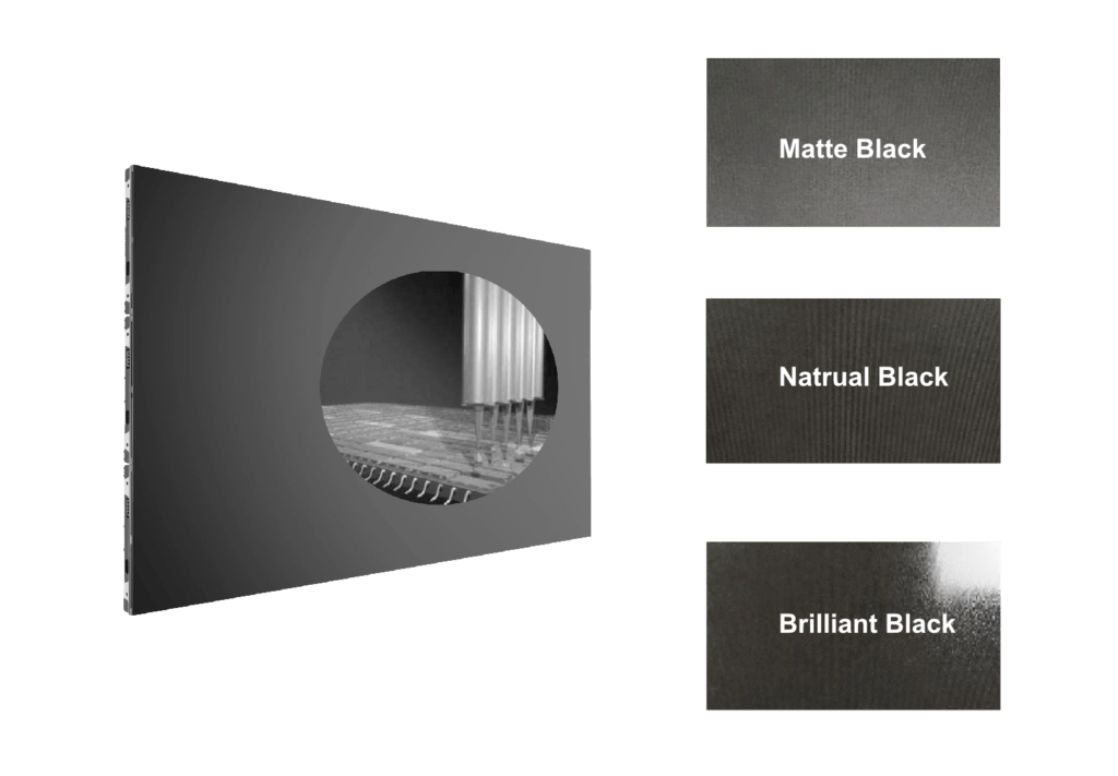
This new and unique technology has a number of advantages over existing technologies such as SMD and DIP LEDs. Due to the small size of the LED chip, the COB system allows for a much higher packing density than SMD (SMT), the result being a more compact array giving better uniformity and higher intensity even at a close distance and greater heat dissipation for better stability, reliability, and lifespan.: COB chip and pin legs are sealed, resulting in better airtightness, higher resistance to external forces, and a smoother, seamless surface. COB has a much higher level of protection against moisture, electrostatic discharge (ESD), damages, and dust with surface protection rated IP65. COB is an integrated package with even light distribution, and the smooth surface makes images appear softer and friendlier to the human eye.
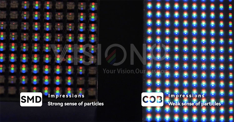
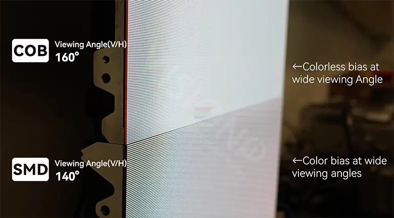
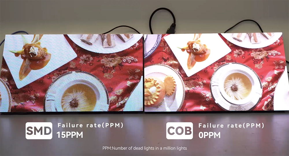
 Superior Durability COB is better at withstanding collisions and the effects of Oil, Damp, Water, Dust, Oxidisation, and dust.
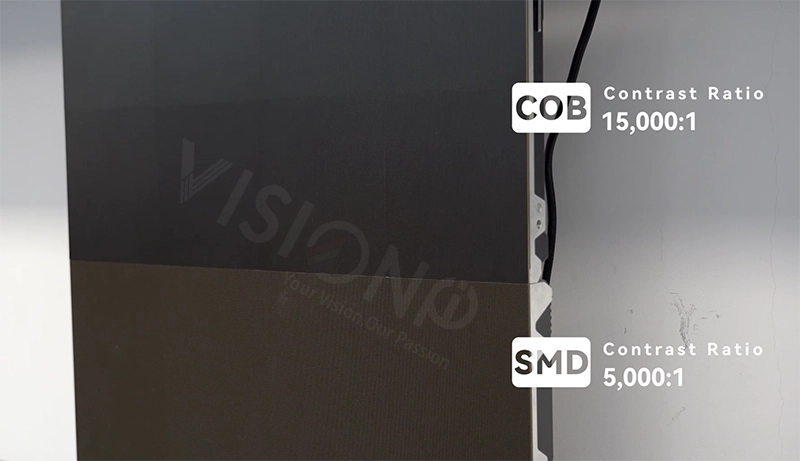
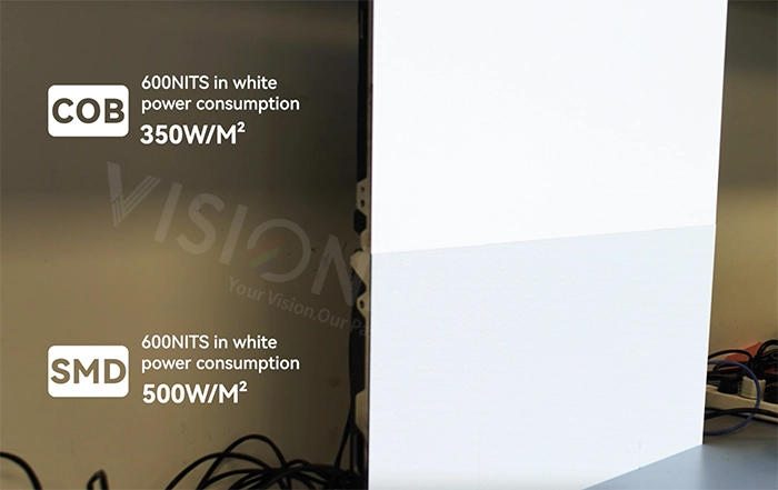
When an LED display is encapsulated in COB, it must be ensured that the lamp is free of defects before refilling. Unlike an SMD package, a single bulb cannot be replaced, so the packaging process is very demanding. (Visionpi’s patented mass transfer technique is a novel approach for transferring millions of micro LED chips accurately. With the mass transfer technology, the UPH of micro & mini LED displays is more than 2.5KK, and the mass production yield rate is more than 99.999%.)
if it is a traditional SMD package, you can disassemble the unit board after a single LED soldering repair. However, when it comes to the COB product, maintenance will affect the surrounding lamps, making it very difficult. Although its protection performance is better, we have to admit that there will still be a certain dead light rate. In this case, the only option is to replace the unit board. generally speacking the cost of maintenance is bout the same with SMD.COB panel is more expensive but with much less possibility of failures. as the cob manufacturing cost is decreasing, now the cob led display’price is very clost to SMD’s, in the future the cost will be lower than SMD.
LC-COB and FC-COB are two types of LED packaging technologies used in Chip-on-Board displays.
LC-COB (wire bonding) has LED chips mounted in parallel on the substrate with electrical connections made from the side of the chip. The chip is attached to the board with an adhesive. Each pad on the device is connected with a fine wire lead that is welded to the pad and to the circuit board. the wire lead would limit the development of finer pixel pitch led display.
FC-COB, on the other hand, has LED chips mounted upside down on the substrate with electrical contacts facing downwards. flip chip COB eliminates wire bonding and simplifies the production process.
Conductive adhesive bonds the chips to the substrate for better thermal and electrical performance.
A reflective layer on the substrate directs light emitted from the LED chips toward the front of the display, providing high brightness.
The flip chip takes a smaller space on the PCB board, providing a larger light-emitting area. The substrate presents a darker black field and higher contrast

Flip-chip COB is the future. Compared with the SMD; GOB Packing technology (GOB VS COB), COB is the next-generation technology advance in COB that improves display quality and durability. It makes the pixels closer, brighter, and more visible from different angles and distances. It also makes the display more reliable, energy-efficient, and resistant to dust, moisture, and collision.COB LED displays are still a popular choice for a wide range of applications such as indoor and outdoor advertising displays, stage backdrops, and event screens, due to their high-quality visuals, energy efficiency, and durability.. In short, COB LED screen technology is a future development trend,the cost will be decreased with the mass transfter technology’s development.
We are a reliable display supplier that offers Mini COB LED displays with three advantages:
Pixel pitch covers P0.4-P1.8 to meet different requirements of users
Quantum Dot COB LED Displays: Revolutionizing Micro-LED Technology
Pixel pitch covers P0.4-P1.8 to meet different requirements of users
COB flexible LED modules merge the compact, high-intensity lighting benefits of Chip On Board (COB) technology with the adaptable, bendable nature of flexible LED modules. This innovative combination allows for the creation of highly durable, uniformly lit, and versatile lighting solutions that can be tailored to fit curved and irregular surfaces without compromising on light quality or intensity.
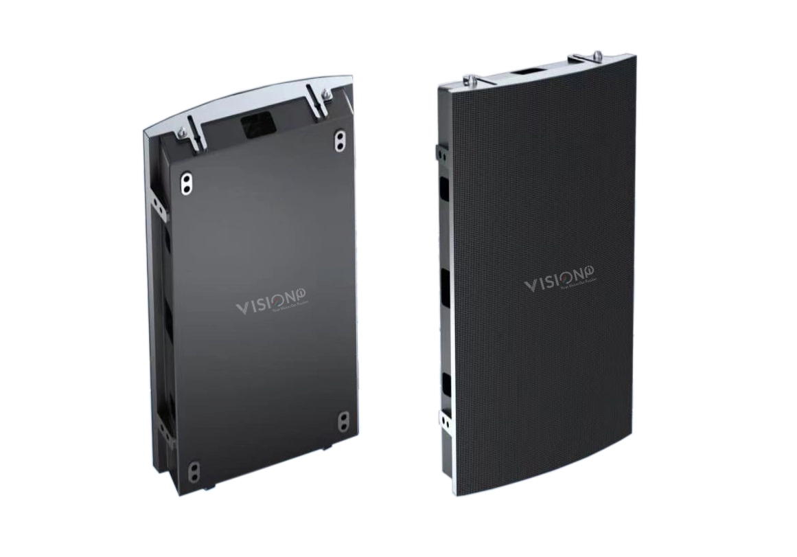
Our flexible COB LED display achieves seamless alignment through a CNC die-cast aluminum cabinet, ensuring high precision and uniformity. The die-casting process provides superior dimensional accuracy and stability, crucial for maintaining flatness in fine-pitch displays. It also minimizes pixel misalignment by maintaining consistent cabinet dimensions.
Additionally, aluminum’s excellent thermal conductivity aids in heat dissipation for high-density LED configurations, extending the display’s lifespan. The robust construction of the die-cast aluminum cabinet enhances durability and resistance to physical stress, making it suitable for various installation environments.
Explore VisionPi’s COB LED Display Module, the pinnacle of cutting-edge technology for OEM applications. As a leading manufacturer, VisionPi offers robust, high-density COB (Chip On Board) LED displays, perfect for creating seamless, high-resolution screens with exceptional durability and performance. Ideal for a wide range of applications from digital signage to sophisticated video walls, discover how our COB LED modules can transform your visual presentations into captivating experiences. Dive into the future of displays with VisionPi’s reliable and innovative solutions
Common cathode low power consuption and high brightness 1500nits cob led modules.